
Researchers at IBM have published a paper at the IEEE’s International Electron Devices Meeting, showcasing a feasible method to embed optical data links into power-efficient 90nm silicon microchips, capable of data rates of 25Gbps.
The IBM silicon nano-photonic chip has both regular (electrical) and optical data connections, with the latter theoretically providing a boost in data transfer speeds and distances, as well as a reduction in power consumption.
IBM’s foray into the field is not the first time that optical data connections have been built into silicon chips, but earlier implementations have been expensive, and requiring specialized production facilities or energy-inefficient lasers. The new nano-photonic technology IBM touting however, was embedded into regular silicon chips by adding new modules to a standard commercial foundry’s fab line.
The photonics researchers say they can use multiple methods for sending and receiving data using pulses of light, including wavelength division multiplexing, which allows for separate recognition of multiple frequencies of light, thereby upping the data transfer rate on a single node.
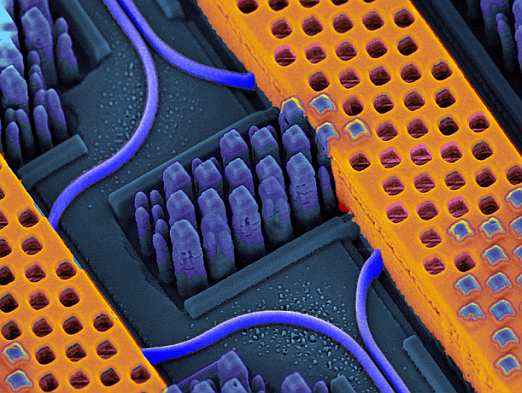
A close-up view of the nano-photonic circuitry, with blue representing the optical waveguides, and the yellow the copper wire for electrical switching.
Current speeds of 25Gbps with the prototype connection can reasonably be expected to improve, with improvements in associated technologies and applied parallelism. IBM’s research into the subject was to find feasible methods of bypassing Moore’s Law, with current day technology.
For now, the silicon photonics chip technology is most expected to help enterprise-scale setups, in server or supercomputer scenarios. IBM has not highlighted a timescale for such a roll-out however. We can expect consumer-aimed hardware to be developed not too long after such adoption though.
An excerpt from the paper presented at the IEEE IEDM event describes the technology:
The first sub-100nm technology that allows the monolithic integration of optical modulators and germanium photodetectors as features into a current 90nm base high-performance logic technology node is demonstrated. The resulting 90nm CMOS-integrated Nano-Photonics technology node is optimized for analog functionality to yield power efficient single-die multichannel wavelength-mulitplexed 25Gbps transceivers.
Source: VentureBeat