
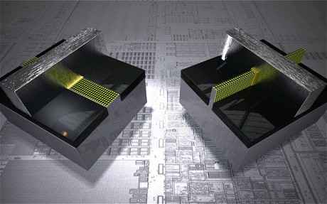
In accordance with its tick-tock model of shrinking processes and new microarchitectures, Intel today announced its 22 nanometer microprocessor, code named “Ivy Bridge”, based on the same microarchitecture as Sandy Bridge. The interesting thing being that these transistors will be the world’s first three – dimensional transistors called Tri-Gate transistors. This is a first since the birth of two-dimensional planar transistors that we have seen since their inception.
According to Intel, the new transistors will use 50 percent less power, conduct more current and improve performance by around 37 percent as compared to the 32-nm planar transistors. At an additional cost of 2-3 percent more, these transistors are expected to have faster switching speeds than the current 32-nm transistors. Chips with these transistors will get into production in the second half of this year and should be available on computers at the start of 2012.
The performance gains and faster switching will allow the processors to be used in mobile handheld devices which operate on low voltages and use lesser energy. So finally Intel can provide some stiff competition to existing players like Qualcomm, Samsung, NVIDIA etc. who have an edge as far as ARM-based processors are concerned which are preferred over the Intel x86 architecture for tablet and mobile devices.
So what exactly does Intel mean by the 3D Tri-Gate transistor. To get the idea, a quick refresher on the working of a transistor should be helpful.
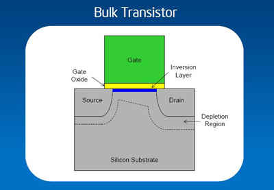
In a normal 2D planar transistor, you have the Source and Drain which are separated by a channel (seen in blue) which when in the ON state allows current to flow and when in OFF state doesn’t allow current flow. These ON/OFF states are determined by the Gate and an insulating layer (seen in yellow). As manufacturing processes start to shrink, problems like leakage of current through the gate begin to appear. Intel countered that by using a High-K materials and Metal Gates to thicken the Gate layers without compromising on performance with their 45-nm chips. But shrinking further does bring up limitations like switching issues.
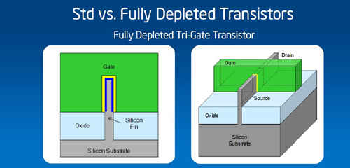
In the 3D Tri Gate design, Intel has pulled up the silicon substrate vertically into the metal Gate called as FinFET (Field Effect Transistor). Due to this vertical expansion of the fin of the substrate, the Gate layer covers three sides of the fin, as opposed to just one flat side (in the 2D planar configuration) thus allowing more current to flow through the transistor and enabling faster switching.
According to Mark Bohr, an Intel senior fellow, this transistor structure will allow Intel to continue the trend of Moore’s Law – which states that the number of transistors placed on an integrated circuit will double every two years.
Intel has put up a great video explaining beautifully the move from 2D planar architecture to 3D Tri-Gate design.
|
|
Also a demo of some machines running on the Ivy Bridge processor.
|
|