
Three words - Tensor Processing Units
Earlier this year, at two different Google events, the company’s CEO spoke at length of the search-engine giant’s significant advances in the field of machine learning, deep neural networks and best-in-class cloud services. Amidst all the bells and whistles, one particular announcement made analysts sit up and take notice. Google’s revelation of TPU, a piece of silicon the company had designed and fabricated to power its machine learning-tuned data centres. Why? Because Google thinks the TPU’s implementation is pivotal to accelerate machine learning by leaps and bounds.
What’s a TPU?
A Tensor Processing Unit is a proprietary chip designed by Google for use specifically for machine learning applications inside its TensorFlow framework – which is an open source software library for machine learning applications. Instead of a CPU or GPU which are designed to undertake a whole host of instruction sets for different software-side tasks and execute them with various degrees of efficiency, a TPU is an ASIC or application-specific integrated circuits chip that’s only designed and programmed for machine learning instructions allowing it to be extremely efficient – certainly more efficient than a CPU or GPU undertaking the same task, according to claims made by Google. The company has only released the following image of what a TPU looks like, and other essential hardware and performance specifications are still a closely guarded secret at Google.
Yes, it’s difficult to decipher a whole lot from this image of a TPU, as released by Google, but this is all we have for now. Wonder what lies beneath that heatsink, and what does the silicon die actually look like. Google has hinted at the fact that the TPU has the same footprint as a hard drive – we don’t know whether they meant it in terms of the unit’s dimensions or power efficiency or both.
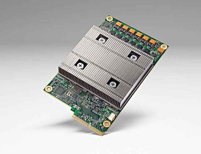
Behold, for this is Google’s own TPU!
The fundamental way in which a TPU differs from a standard CPU (from Intel or AMD) or GPU (from NVIDIA or AMD) is its computational efficiency. Where a CPU and GPU is designed on a 64-bit architecture, experts are of the opinion that Google’s TPU will most likely be running on 8-bit or 16-bit architecture which is far less precise in comparison. The advantage of sticking to an 8-bit or 16-bit cycle allows more logical circuits to be physically installed on the chip, allowing TPUs to calculate more operations per second and thereby be more efficient (in general and precise terms) than CPUs or GPUs.
Through TPUs and advancements in machine learning, Google claims it has advanced its hardware competency by up to three generations (or cycles) of Moore’s Law. This is critical to give the company and its services a decisive edge over competition, as machine learning is used by over 100 product teams in Google – from Natural Language Processing (voice search), Smart Reply in Inbox, Street View in Maps, and a whole lot more.
Beyond the marketing hype
Of course, TPUs are just plain and simple ASICs, at the end of the day, whatever Google may call them. There’s a lot of merit in designing and manufacturing application-specific hardware as much as possible, to drive up efficiency of the system overall. Bitcoin mining is a very specific activity, requiring the system to do it ever more efficiently, for instance. The better a circuit’s design to mine bitcoin, obviously the better it will perform.
Google’s TensorFlow framework’s open source, designed for machine learning apps
While Google hasn’t really designed and created a piece of silicon from scratch before – at least from what’s public knowledge – it has a history of tinkering with commercially purchased, off the shelf hardware to best suit its work environment. Remember back in 2009, when news first broke about a custom-made Google server with a unique onboard UPS battery unit fitted onto the board itself to ensure power efficiency and redundancy? The company has understood long ago that the success of its critical software-driven infrastructure depends closely on efficient hardware systems powering it all.
Let’s get one thing straight – Google’s not suddenly becoming a silicon provider like NVIDIA or Intel. That’s not its traditional strength. Which means it’s not going to pose an immediate threat to companies that fabricate and manufacture silicon chips. But – and this is an important but – Google has demonstrated very clearly that through TPUs it plans to enable the Google Cloud Platform and TensorFlow ecosystem to race far ahead of its competitors.
In fact, analysts believe that NVIDIA with its Pascal-based GPU is probably the best equipped hardware platform for Deep Learning AI. That’s right, not just used for calculating polygons and graphics, NVIDIA Pascal-based GPU stacks are great at numerical floating point calculations at a record pace. In fact, NVIDIA’s P100 is considered as a behemoth of the machine learning / AI industry, primarily used for training or increasing a system’s learning capability – a far bigger challenge in machine learning parlance than ‘inferencing’ or predicting an outcome. Google hasn’t confirmed it yet, but word on the street is that TPUs are most likely being used for inferencing purpose in the company’s machine learning endeavours.
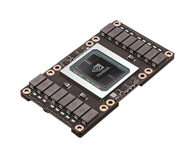
The NVIDIA P100 chip
Healthy competition
Google obviously has a lot to share about TPUs, and our guess is that it’s deliberately holding most of its secret hardware cards close to its chest – it has every right to do so. What’s happening as a result is that the AI / deep learning / machine learning industry as a whole is trying to ramp up their operations – both on the hardware (Intel, NVIDIA, IBM, etc) and cloud-software side (Microsoft Azure, Amazon Web Services and EC2, etc) of things. This healthy competition between these industry heavyweights will ensure the pace of innovation doesn’t lose steam, that in fact it picks up by several notches, and that’s a good sign for the future of machine learning and evolution of AI.
TPUs are a sign of things to come. It’s a signal that the machine learning market at large is moving from an exploratory phase – where it was okay for companies to throw money at unearthing effective, accurate solutions – to a commercialization phase – where it’s now imperative for companies to find cost-effective, ever-efficient solutions on top of being accurate. This means startups spawning in the machine learning / neural networks space now have options to choose from on what they want to do. The potential of FPGAs or Field Programmable Gate Array – which allows customers to reconfigure the chip after it’s manufactured – also becomes extremely important, giving stalwarts like Intel and Microsoft something to pit against Google’s TPU prowess.
FPGAs can give TPUs stiff competition
In the race to develop the best AI, on the foundation of highly-efficient machine learning systems, power usually resides with those who have the most data. And if there’s one thing about Google that we know for sure, something that even Facebook will begrudgingly agree to, is that they have a LOT of data.
This article was first published in November 2016 issue of Digit magazine. To read Digit's articles first, subscribe here or download the Digit e-magazine app for Android and iOS. You could also buy Digit's previous issues here.
Jayesh Shinde
Executive Editor at Digit. Technology journalist since Jan 2008, with stints at Indiatimes.com and PCWorld.in. Enthusiastic dad, reluctant traveler, weekend gamer, LOTR nerd, pseudo bon vivant. View Full Profile


