iPhone 5 A6 SoC reverse engineered, reveals rare hand-made custom CPU, and tri-core GPU

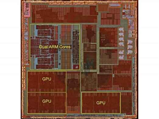
Apple still hasn’t said a word about the new A6 SoC within the iPhone 5, but no matter: Chipworks — a company that specializes in reverse engineering computer chips — has now completed its initial analysis of the A6, and the results are very interesting indeed. The A6 features a custom, in-house, laid-out-by-hand dual-core design (pictured above) that is neither a Cortex-A9 or A15, and a tri-core GPU.
By far the most exciting aspect of this news is the fact that the A6′s dual ARM CPU cores have been manually laid out — an approach that used to be the norm, but which is now almost unheard of outside of Intel (even AMD has given up). Today, chips are nearly always laid out using advanced, CAD-like software — the designer says he wants X cache, Y FPUs, and Z cores, and the software automagically creates a chip. Hand-drawn processors, on the other hand, are painstakingly laid out by chip designers. This approach obviously takes a lot longer (and is a lot more expensive), but if it’s done correctly the end result can be a lot faster.
In the case of the A6, which benchmarks very well indeed, it would seem that its chip design department knows what it’s doing. This probably isn’t a big surprise, though, when you remember that Apple acquired PA Semi back in 2008, for the purpose of bolstering the capabilities of its mobile devices. PA Semi was founded by one of DEC’s lead chip designers and has over a hundred engineers who have worked on chips at Intel and AMD, among others. I wouldn’t be surprised if PA Semi has been working on the hand-made A6 since its acquisition.
As far as the custom core’s actual functionality, we still don’t have much to go on. At this point, it still looks like the A6′s CPU core is similar to Qualcomm’s Snapdragon S4 Krait — roughly doubling the performance of the Cortex-A9 chip, while still remaining very power efficient.
GPU, die size, manufacturing process, and more
Now, the tri-core GPU. Chipworks says that the GPU cores Imagination Technologies PowerVR cores — but beyond that, we don’t know exactly what they are. Judging by Apple’s boast of “2x the performance,” we are probably looking at the same SGX543 GPU cores found in the A5 and A5X SoCs, but at a higher clock speed.
Beyond the hardware specs, Chipworks’ reverse engineering also confirms that the A6 is produced using Samsung’s 32nm HKMG process, and that the total die size is 9.7mm by 9.97mm (96mm2). This is actually quite large, when you bear in mind that the 32nm A5 only had an area of 71mm2. The 26-square-millimeter difference is mostly accounted for by the larger, hand-made CPU cores in the A6, and the addition of a third GPU core.
Unfortunately, beyond the CPU and GPU cores, Chipworks hasn’t labeled any other SoC features. We know that most of the right and bottom edges are the interface, and the silver squares on the mid-right are PLLs — but beyond that, the other squares are unknown. If you recognize any of the features, leave a comment below.
For lots and lots of pretty photos, be sure to hit up Chipworks. Not only have their engineers reverse engineered the A6, they’ve also taken a look at the Sony camera sensor — and over on iFixit, Chipworks has shared some die shots of the Qualcomm MDM9615 radio and the Broadcom WiFi chip.

Copyright © 2010 Ziff Davis Publishing Holdings Inc