Samsung Delays 1.4nm Chips to 2029, Doubles Down on Advanced 2nm and 4nm Foundry Tech
Samsung Electronics is recalibrating its semiconductor foundry roadmap, putting the spotlight squarely on refining its 2 nm (SF2) process family while putting its next-generation 1.4 nm node on the back burner, at least for now.
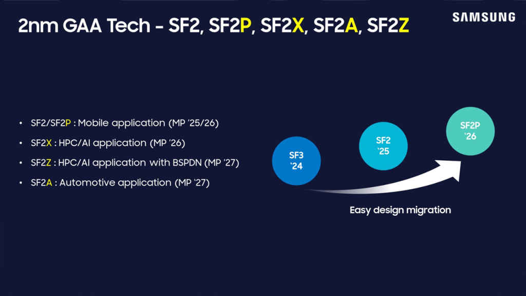
At its latest SAFE Forum for partners, the Korean tech giant unveiled the SF2P+ process, the third iteration of its 2nm technology. The new node is built upon an advanced optical shrink of SF2P, promising a 20 to 30 percent improvement in performance over previous generations, while maintaining the same transistor structure. Samsung plans to bring SF2P+ into mass production in 2026.
This marks a strategic shift for the foundry arm of Samsung Electronics. Rather than chasing aggressive node scaling timelines, the company is prioritising yield stability and competitiveness, particularly as it looks to win back customers such as NVIDIA and Google who’ve drifted to rivals like TSMC in recent years.
Optic Shrink approach: smaller footprint, familiar design
The SF2P+ process is an evolution of the second-generation SF2P (2nm Performance) node, which itself offered measurable gains over the first-gen SF2. According to Samsung, SF2P delivered a 12 percent improvement in performance, a 25 percent drop in power consumption, and an 8 percent area reduction over SF2. That process is now being promoted to external customers, including domestic AI semiconductor startup Revelion.
SF2P+ builds on that with a technique called Optic Shrink. It’s a lithographic refinement that rearranges and reduces the size of an existing transistor layout without changing the underlying transistor structure. The result: better performance and reduced die area, without introducing significant design complexity. A partner company representative likened it to reducing a numerical figure by simply shrinking it, “if the existing semiconductor is the number 1, then the shrink is a smaller 1.”
This pragmatic approach has a distinct advantage. Since the optical shrink doesn’t require a fundamental redesign of the transistor architecture, it can be brought to production faster and at lower risk. This is especially relevant as Samsung Foundry tries to climb back into favour with fabless chipmakers.
1.4 nm roadmap pushed to 2029
The pivot toward refining current-generation nodes means Samsung’s original plans for a 1.4 nm (or 14Å) process have taken a backseat. The 1.4 nm node, previously projected to enter mass production by 2027, is now scheduled for 2029. The delay was addressed during the SAFE Forum and framed as a strategic decision rather than a setback.
A Samsung spokesperson said the focus will be on “stabilising existing processes such as 2 nm and 4 nm and improving yields” rather than fast-tracking the move to the next frontier. That sentiment was echoed by a semiconductor industry insider at the event, who summarised the message as a bid to “create an ecosystem where customers who used Samsung Foundry can find Samsung again.”
Rebuilding customer trust through mature nodes
As part of its renewed effort to court existing customers, Samsung is also putting significant weight behind its 4nm offerings, especially the SF4U process. The “U” stands for “Ultra,” reflecting its focus on power efficiency improvements. Unlike the 2 nm line, which uses GAA (gate-all-around) transistors, SF4U is based on the more mature FinFET architecture.
SF4U is being optimised for use cases in mobile application processors, automotive SoCs, and AI accelerators. Design houses that partner with Samsung see this as a positive move, suggesting that Samsung’s foundry business is shifting focus in the direction of strengthening the existing process around the four nanos that have entered the mature process.
This maturity may give Samsung a steadier platform to build on in its competition with TSMC, which continues to lead the global foundry market. With TSMC’s N3 and N2 processes in various stages of rollout, Samsung’s commitment to boosting performance and yield within its 4nm and 2nm lines could give it a sharper competitive edge where it matters most, volume production and reliability.
Early 2 nm GAA chips in the pipeline
While the SF2P+ process isn’t due for mass production until 2026, the second-generation SF2P is scheduled to hit production lines next year. It’s expected to play a key role in Samsung’s own Exynos roadmap, including the prototype production of the Exynos 2600, which will be built using the 2nm GAA node.

Samsung is currently targeting a yield rate of around 50 percent in the coming months for its early 2nm GAA runs. That figure is expected to climb steadily, with meaningful volumes likely by late 2025.
Separately, there are murmurs that Qualcomm may tap Samsung to fabricate a special Galaxy S26-exclusive version of the Snapdragon 8 Elite Gen 2 on its 2nm GAA node. The chip is reportedly being tested under the codename ‘Kaanapali S’.
Steady progress, not a sprint
Samsung’s foundry strategy appears to be shifting from a race for nanometres to a campaign for stability and customer confidence. The decision to delay 1.4 nm in favour of refining 2 nm and 4 nm nodes may disappoint some observers, but it reflects a broader understanding that success in advanced manufacturing is about delivering consistent results at scale.
If Samsung can prove that its SF2P and SF2P+ nodes offer reliable performance and solid yields, it may finally begin to reclaim lost ground in the fiercely competitive contract chip manufacturing sector.
But the real test lies ahead. With mass production of 2 nm chips drawing near and customer expectations high, 2025 could be the year that decides whether Samsung’s strategic patience pays off.
Source: ZDNet