NanoStack explained: Did IBM really build a 0.7nm chip?
IBM unveils NanoStack, world's first manufacturable sub-1nm chip technology
NanoStack stacks transistors vertically instead of shrinking them flat
Nearly 100 billion transistors fit on a fingernail-sized chip, production 5 years away

For 25 years, every faster phone and thinner laptop’s story has been pretty much the same. It involved shrinking the transistor, cramming more of them onto a semiconductor chip, rinse and repeat the process every couple of years. It’s what’s defined Moore’s Law for 60+ years – and now IBM says it has found a new way to prolong it.
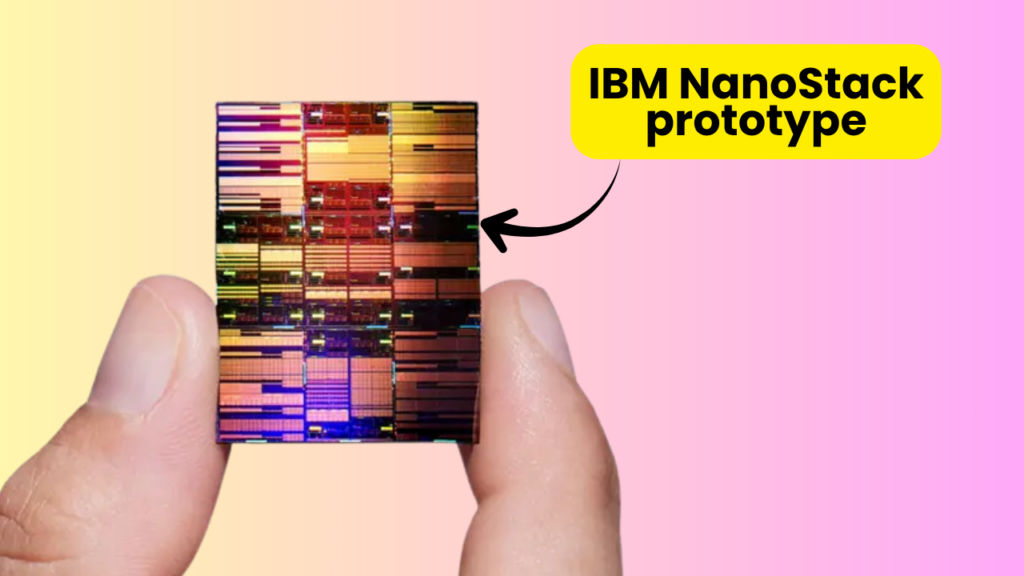
IBM has unveiled a prototype it calls NanoStack, which is a “0.7-nanometre” or “7-angstrom” technology – the first sub-nanometre chipmaking process IBM claims is manufacturable. That’s what they essentially proved with the NanoStack prototype, duh.
IBM shares jumped more than 6% on the news, which means investors really liked the announcement. But here’s the interesting thing – IBM isn’t shrinking transistors at all. So what’s going on here?
Reality check on “0.7nm”
Well, the number is marketing. The “0.7nm” label doesn’t describe any physical feature on the chip – node names stopped being literal measurements years ago. By IBM’s own account, the spacing between transistors has hovered around 40nm for a long time and isn’t shrinking anytime soon – definitely not in NanoStack either.
This matters for how you contextualise chip-related information, including the one inside your current phone or laptop, for example. When Apple’s A19 Pro (in the iPhone 17 Pro) is called a “3nm” chip, or the Intel 18A powered Panther Lake laptops is said to have a “1.8nm” chip, remember those are generation labels – not the width of anything you could measure on the chip’s physical surface.
Therefore, IBM’s “0.7nm” chip technology is best read as something that’s probably two full generations beyond the 2nm chips arriving in flagship phones right now, and not as a transistor on the IBM chip’s surface that’s literally sub-nanometre.
So what chip has IBM actually built?
According to IBM’s research blog, NanoStack’s like a fingernail-sized chip holding nearly 100 billion transistors. To put 100 billion in perspective using the chips in your pocket and on your desk:
- The A17 Pro in the 2023 iPhone 15 Pro (which I’m currently using) packed 19 billion transistors.
- The A19 Pro in today’s iPhone 17 Pro is estimated in the 25–30 billion range.
- The Intel 18A Panther Lake chip inside a laptop has roughly 3-5 billion transistors.
NanoStack roughly doubles the density of the 2nm-class technology IBM demonstrated back in 2021. Compared to that 5-year-old chip tech, IBM claims the NanoStack prototype delivers a 50% performance bump and up to 70% better energy efficiency.
IBM’s pitch is fitting close to a hundred billion transistors into a fingernail-sized slice aimed not at workstations or high-powered server chips, but instead at small, battery-powered mobile devices.
Transistor layout: How IBM differs from Intel and TSMC
In order to understand what IBM has demonstrated with NanoStack, and how it’s potentially different from how Intel or TSMC builds their chips, you need to understand how transistor architecture works inside a semiconductor chip.
For decades, transistors inside a chip have been laid essentially flat – side by side on a single plane, like houses on a street. The whole industry, including IBM, recently upgraded from older “FinFET” transistors to a newer design called Gate-All-Around (GAA) to build better chips, and that’s what TSMC’s 2nm process and Intel’s 18A process essentially use. But GAA is still fundamentally a flat layout. You make things denser by packing the houses closer together, by thinning down the streets.
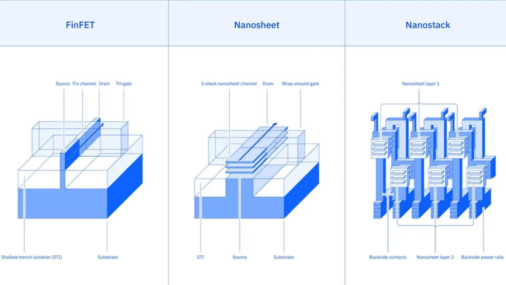
NanoStack builds upward or vertically instead of just sideways or horizontally. It vertically stacks transistors in offset layers – think of it as going from a row of bungalows to a row of duplexes or small multi-storeyed buildings. The same plot of land now gives you more space to build – vertically, not horizontally.
IBM hasn’t built NanoStack out of nowhere. Credit where credit’s due, the company was first to demonstrate scaled GAA in 2021 – the same architecture that TSMC, Intel and Samsung went on to build their own versions of, and which is reaching phones and laptops this year. With this in mind, NanoStack is IBM’s attempt to show the next direction the semiconductor industry is heading toward – vertically stacked transistors (the broader industry calls the family “CFET”).
TSMC is ramping 2nm (N2) production now, the process behind Apple’s upcoming A20, with 1.6nm (A16) and 1.4nm (A14) expected very soon on its roadmap. Intel said just last week that its 18A-P process (1.8nm-class) for performance tuned chips entered “risk production,” the testing phase right before commercial manufacturing. NanoStack sits well beyond all of these on the timeline.
When to expect real products?
While NanoStack is a milestone for IBM and the semiconductor industry as far as prototypes go, stacking transistors introduces a huge yield problem – a fact that IBM’s own researchers flagged. Because when you build a second layer on top of the first, the whole chip essentially gets bricked if any one of the two layers fails.
Since manufacturing semiconductor chips always produces defective chips, creating two layers of transistors essentially means doubling the chances of failure. Solving this problem effectively where chip wafer yields are produced at high volume – because it directly impacts the cost of the future phone or laptop you will buy – is the most difficult challenge now ahead of IBM and the industry.
When will phones or laptops based on this new chip technology reach your hands? Not for at least five more years, suggests IBM, so think around 2030 or later. IBM expects chips produced on NanoStack tech to be first available for smartphone or AI chiplets, before percolating down the value chain.