
Introduction:
The Terasic DE-10 Nano is a development kit that contains a Cyclone* V device. The Cyclone V contains a Hard Processor System (HPS) and field-programmable gate array (FPGA) with a wealth of peripherals onboard for creating some interesting applications. One of the most basic things to accomplish with this system is to control the LEDs that are physically connected to the FPGA. This tutorial will discuss four different methods for controlling the LEDs using the command line, memory mapped IO, schematic, and Verilog HDL.
Whether you are an application developer, firmware engineer, hardware engineer, or enthusiast, there is a method suited for you.
Prerequisites:
There are a wealth of datasheets, user guides, tools, and other information available for the DE-10 Nano. It is encouraged to review this documentation to get a deeper understanding of the system. For this tutorial, please download and install the following first:
01: Intel® Quartus® Prime Software Suite Lite Edition for Cyclone V – http://dl.altera.com/?edition=lite
02: Install EDS with DS-5 – http://dl.altera.com/soceds/
03: Install Putty (Windows* Users) – http://www.putty.org/
04: Install WinScp (Windows Users) – https://winscp.net/eng/download.php
05: Install the RNDIS Ethernet over USB driver (Windows Users) – See Terasic DE10 Nano Quick Start Guide Section 3
06: Download DE-10 Nano Resources – http://www.terasic.com.tw/cgi-bin/page/archive.pl?Language=English&CategoryNo=205&No=1046&PartNo=4
Method #1 – Command Line:
Out of the box, the DE-10 Nano HPS is pre-configured to boot a Linux* image and the FPGA is pre-configured with the Golden Hardware Reference Design (GHRD). This means you have a complete system and can get started exploring right away by simply applying power to the board. The most basic method to control an LED using the DE-10 Nano HPS is with the file system. This method lends itself well to the scripters out there that want to do something basic and work at the filesystem level. This can be easily illustrated using the serial terminal. To begin, perform the following:
01: Connect a Mini-B USB cable from the host to the DE10 Nano USB UART (Right Side of board)
02: Open a serial terminal program
03: Connect using a 115200 baud rate
04: Login as root, no password is needed
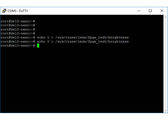
05: Turn on the LED
echo 1 > /sys/class/leds/fpga_led0/brightness
06: Turn off the LED
echo 0 > /sys/class/leds/fpga_led0/brightness
Method #2 – C Based Application:
Another method to control the LEDs using the HPS, is to go lower level and develop a Linux application that accesses the memory mapped regions in SDRAM exposed by the FPGA that control the LEDs. The HPS can access this region using the Lightweight HPS2FPGA AXI Bridge (LWFPGASLAVES) that connects to the Parallel IO (LED_PIO) area. The C based application will map this region into the user application space, toggle all 8 LEDs every 500ms for a few times, unmap the region, and exit. We will develop the application using the Eclipse DS-5 IDE. To begin, perform the following:
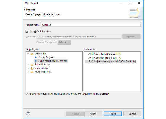
01: Open Eclipse DS-5
02: Create a New Project
02a: File->New->C Project->Hello World Project
02b: Enter a project Name
02c: Select GCC 4.x [arm-linux-gnueabihf) Toolchain
02d: Click Finish
03: Delete the generated Hello World code
04: Add Preprocessor Includes & Defines
#include <stdio.h>
#include <unistd.h>
#include <fcntl.h>
#include <sys/mman.h>
#define ALT_LWFPGASLVS_OFST 0xFF200000
#define LED_PIO_BASE 0x3000
#define LED_PIO_SPAN 0x10
05: Add main() function
int main(void)
{
unsigned long *led_pio;
int fd;
int i;
fd = open("/dev/mem", (O_RDWR | O_SYNC));
//Map LED_PIO Physical Address to Virtual Address Space
led_pio = mmap( NULL, LED_PIO_SPAN, ( PROT_READ | PROT_WRITE ), MAP_SHARED, fd, (ALT_LWFPGASLVS_OFST + LED_PIO_BASE) );
//Toggle all LEDs every 500ms a few times
for (i=0; i < 10; i++)
{
*led_pio ^= 0xFF; //Bit0=LED0 … Bit7=LED7
usleep(1000*500);
}
//Unmap
munmap(led_pio, LED_PIO_SPAN);
close(fd);
return(0);
}
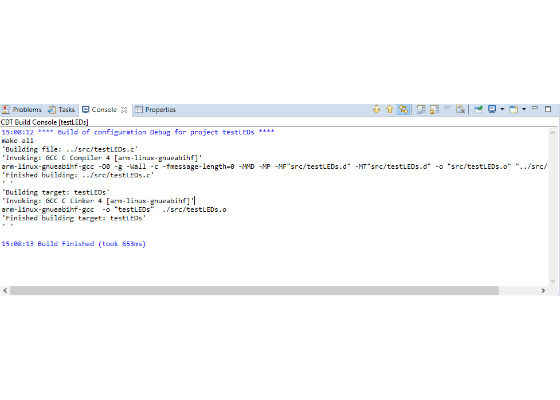
06: Build the Project
Project->Build Project
07: Test out the application
06a: Connect a micro USB cable from the host to the DE10 Nano USB OTG Port
06b: Use scp to transfer the application to the DE10 Nano at root@192.168.7.1
06c: Run the application from the serial terminal ./<applicationName>
Methods #3 & #4 – Schematic and Verilog HDL:
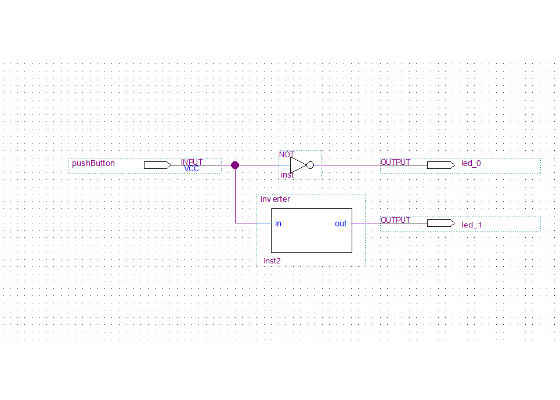
So far we have been controlling the LEDs connected to the FPGA from the HPS using the command line and a C based application. Now let’s discuss controlling the LEDs directly using just the FPGA logic. In this design, we will turn on/off 2 LEDs when a pushbutton is pressed/released respectively. It should be noted that the pushbutton is pulled up and the LEDs are active high so an inverter is used to get the desired behavior when the button is pressed/released. We will use a schematic based approach to create the logic to control the first LED and a Verilog HDL approach to create the similar logic to control the second LED. We will create the design using the Intel® Quartus® Prime Software Suite Lite Edition software. To begin the project, perform the following:
01: Open Quartus Prime Lite
02: Create a New Project
02a: File->New->New Quartus Prime Project->Next
02b: Enter Project Name->Next->Empty Project
02c: Click Next
02c: Name Filter->5CSEBA6U23I7->Finish
03: Create a New Schematic File
03a: File->New->Block Diagram/Schematic File
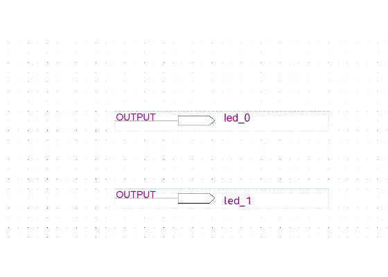
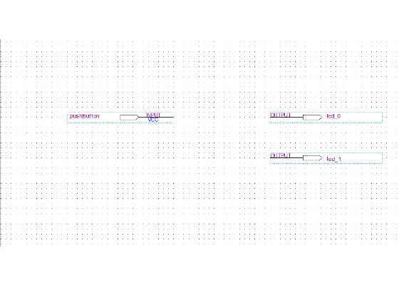
04: Add LED Output Pins
04a: Right Click->Insert Symbol->primitives->pin->output
04b: Right Click->Insert Symbol->primitives->pin->output
04c: Right Click on output pin->Properties->Name=led_0
04d: Right Click on output pin->Properties->Name=led_1
05: Add Push Button Input Pin
05a: Right Click->Insert Symbol->primitives->pin->input
05b: Right Click on input pin->Properties->Name=pushButton
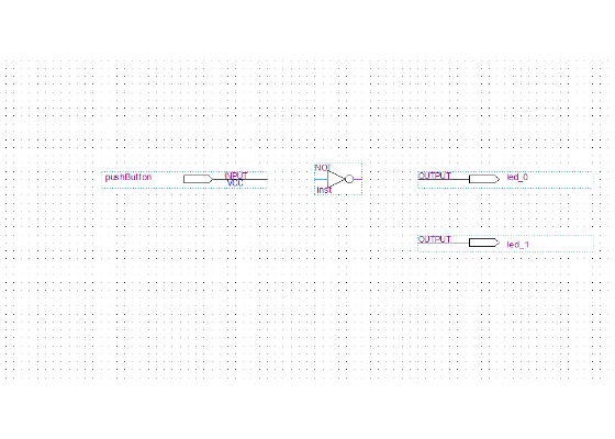
06: Add Inverter
06a: Right Click->Insert Symbol->primitives->logic->not
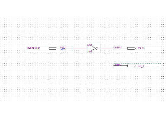
07: Connect Everything Up
07a: Connect pushButton to Inverter Input
07b: Connect Inverter Output to led_0
08: Create a New Verilog HDL File
08a: File->New->Verilog HDL File
08b: Enter Verilog Code
module inverter (
input in,
output out
);
assign out = !in;
endmodule
08c: Save File
08d: Update Symbols
File->Create/Update->Create Symbols From Current File
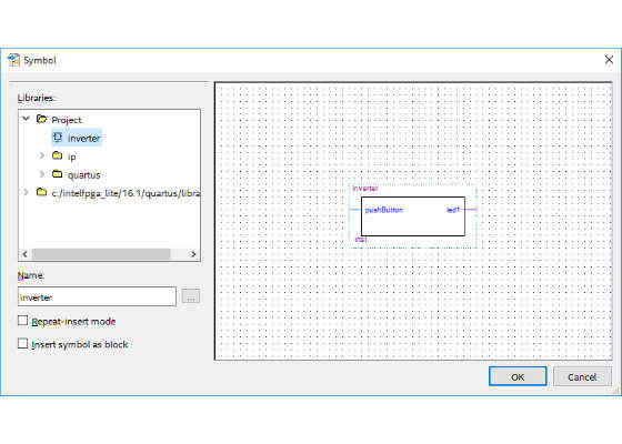
08e: Add Verilog Module to Top Level Schematic
Right Click->Insert Symbol->inverter->Click Ok
08f: Connect pushButton Input to Inverter Input
08g: Connect Inverter Output to led1 Output Pin
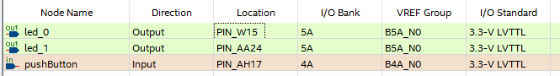
09: Assign Inputs and Outputs to Physical FPGA Pins
09a: Processing->Start->Start Analysis & Elaboration
09b: Assignments->Pin Planner
led0->Location=PIN_W15, I/O Standard=3.3-V LVTTL
led1->Location=PIN_AA24, I/O Standard=3.3-V LVTTL
pushButton->Location=PIN_AH17
10: Compile Project
10a: Start->Start Compilation
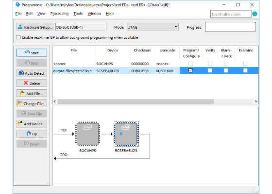
11: Program the FPGA
11a: Connect mini USB cable to JTAG USB Blaster port (near HDMI connector and Blue LED)
11b: Click Tools->Programmer
11c: Click Hardware Setup->Currently Selected Hardware->DE-SoC
11d: Click AutoDetect->5CSEBA6
11e: Click on 5CSEBA6U23 Chip Picture
11f: Click Change File-><project directory>\output_files\yourFile.sof
11g: Click Program/Configure checkbox
11h: Click Start Button
12: Test out the design
12a: Push and hold the right pushbutton and led0 and led1 will turn on
12b: Release the pushbutton and the LEDs will turn off
Summary:
The DE-10 Nano has a lot to offer the engineer from its capabilities, variety of tools, programming methods, and documentation. This tutorial showed four different methods for controlling the LEDs that utilized the HPS and FPGA using the available tools. You can take all of these concepts to the next level when you begin your next project with the DE-10 Nano.
For more such intel IoT resources and tools from Intel, please visit the Intel® Developer Zone
✅ Thank you for completing the survey!
Source: https://software.intel.com/en-us/articles/exploring-the-hps-and-fpga-onboard-the-terasic-de10-nano