TSMC has started working on development of the 2nm lithography process
TSMC has started working on development of 2nm process
Work on 3nm has stalled due to unavailability of instruments
TSMC's 5nm production lines are currently at capacity

TSMC has allegedly begun work on its 2nm lithography, according to industry insiders. The report, however, comes via WCCFTech who report that amidst a shortage of components, TSMCs refinement of 3nm lithography has slowed down, so the company is using the time to work on the next big/small thing.
Earlier this month, TSMC reported that its 5nm production lines were working at full capacity, leading us to believe that 5nm chips may not be farther away than the end of the year. TSMCs CoWoS Interposer lines are also currently at capacity, given that the demand has suddenly skyrocketed over the last few weeks. Companies like Nvidia, HiSilicon, AMD and even Broadcomm have increased their demands so that they can use them in high bandwidth applications like AI accelerators and ASICS.
TSMCs 5nm fabrication lines are also operating at capacity, possibly to meet the demands of upcoming processors. We expect Apple to move to the 5nm process for the A14 Bionic chip that will be a part of the 2020 iPhone. Additionally, AMD has already announced that its Zen 4 architecture will be based on the 5nm node, and the company expects it to be available starting 2022. The current architecture, Zen 2, is based on the 7nm process and according to AMD's own roadmap, Zen 3 is expected by the end of 2020, with the architecture achieving major permeation in the markets by 2021.
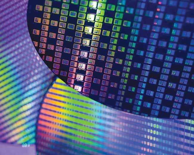
Needless to say, even with a shortage of equipment to work on the 3nm process, TSMC definitely has its hands full between the production of 7nm and 5nm chips. According to DigiTimes, the 5nm process will be based on the Extreme UltraViolet or EUV method. This method employs a laser with a wavelength of 13.5nm to etch the gates onto the silicon wafer. The reduction in the size (to 7nm or 5nm) is achieved using stencil overlays. EUV has been unviable up until now due to the extreme power requirements of the laser, however, it would appear that companies like TSMC and Samsung have both figured out how to work around that problem.
As we start to move towards chipsets utilizing the 5nm process, it's only logical for TSMC to work on the next step of the miniaturization process. Due to the COVID-19 outbreak, TSMC has had to face delays and shortage of various equipment required for working on the 3nm node, but instead of just waiting, the company has become work on designing the 2nm lithography. This could involve a new laser with an even lower wavelength of light, or it could just be achieved using pairs and combinations of stencils.