AMD HD 8000 specs leak, point to major performance boost

Last week, spec sheets on AMD’s Radeon HD 8000 series leaked out to the press. The chart shows the two upcoming graphics cards that would theoretically replace AMD’s HD 7870 and 7850. The new HD 8000 family, codenamed Sea Islands, will be AMD’s first major refresh of its GCN (Graphics Core Next) architecture that debuted last year. The two cards we have information on are based on the Oland GPU, and would replace the Pitcairn family. Like the 7870/7850, the new GPU is built on a 28nm process at TSMC.
 Survey
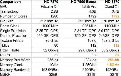
With leaks like this, there’s always the question of whether or not the data is valid. We’ve gone through and crunched some numbers, and figured out a few metrics that the original table doesn’t show. Here’s the original first, without any additional data.

Chart courtesy of Videocardz
These improvements align nearly perfectly with what we’d expect a next-gen architecture to deliver in the same price bracket. Memory bandwidth bumps upwards thanks to the use of faster GDDR5 RAM, pixel fillrates are up slightly, texture fillrates improve significantly. Since we know how many Render Output Units (ROPs) and Texture Mapping Units (TMUs) are in the 7870, we can extrapolate what the 8870 is packing in those departments.

We’ve added data from the HD 7950 Boost Edition and included current prices for Radeon cards as seen on Newegg. Columns labeled in orange reflect our extrapolations on the new core. The math fits, perfectly, in every example. The Radeon HD 8870 is built like a Radeon 7950.
Note that I said “built like,” not “equivalent to.” The current Radeon HD 7950 is a cut down Radeon 7970; AMD and Nvidia both improve yields by selling cards with certain function blocks disabled. This allows them to recoup a return on products that aren’t quite perfect, rather than tossing them on the slag heap. As a result, the 7950′s die is the same size as the 7970′s, despite the disparity in core count.
This data suggests that AMD felt the 7950 presented an ideal performance balance for a midrange card and opted to scale the chip downwards with a few changes made to decrease die size. The 384-bit memory bus is gone, though the faster GDDR5 memory compensates well for this. On the whole, the 8870 should be faster than the 7950 it replaces thanks to a higher core clock.
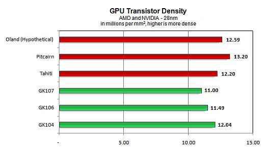
There are other reasons why this shift makes sense. Transistor densities across AMD and Nvidia are typically quite similar when comparing them at the same node.

Oland’s 3.4B and 270mm sq die size are right where we’d expect them to be.
Just because the Radeon 8870 is specced like a 7950 doesn’t mean it’ll perform like one. AMD will have tweaked the architecture to improve performance and power efficiency; the lower TDP is proof enough of that. This data suggests that AMD is pursuing an evolutionary strategy with the HD 8K GPU. When the company built the HD 6000-era Barts and Turks chips, they were a continuation and enhancement of the highly successful HD 5000 core. Cayman, the chip at the heart of the HD 6900 family, was the new architecture.
AMD could be planning to open a major new front with the high-end HD 8900 parts, but we’ll have to wait and see. GCN remains an excellent architecture, and AMD has enough on its plate trying to deal with bringing new SoCs to market — the company may have chosen a single GPU strategy to divert engineering resources where they’re needed most.
Copyright © 2010 Ziff Davis Publishing Holdings Inc
