Intel launches Panther Lake, first AI PC chip on 18A
New US-made 18A process node rivals TSMC's advanced processes
Fab 52 begins high-volume production to support scalable AI future

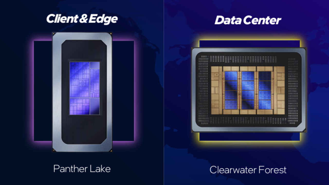
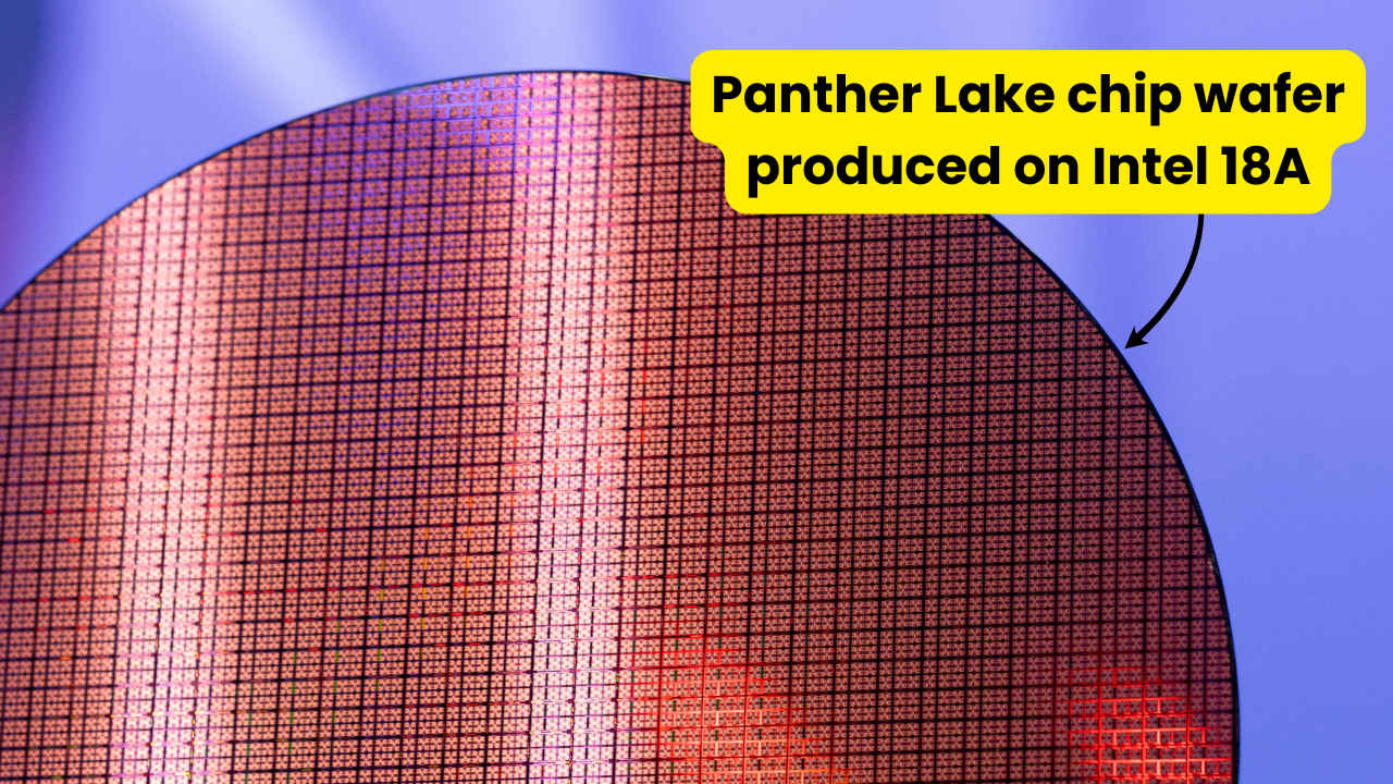
Intel took the wraps off its third-generation of AI PC chip, Intel Core Ultra series 3 – codenamed Panther Lake. It’s Intel’s next processor update to feature in laptops starting in 2026, and the first to be built on its new 18A semiconductor process. Set to power a wide range of AI-enabled PCs and edge devices, Intel Core Ultra series 3 or Panther Lake chips will begin shipping later this year, with high-volume production ramping at Intel’s newest manufacturing facility, Fab 52, in Chandler, Arizona.
Intel also offered an early look at Clearwater Forest – its first Xeon server processor based on 18A – scheduled to launch in the first half of 2026. These announcements were made as part of the company’s 2025 Tech Tour, which Digit attended, marking a key milestone in Intel’s multi-year roadmap to regain leadership in process technology and semiconductor manufacturing. Both chips are being produced at Fab 52, Intel’s most advanced factory to date and part of its $100 billion US expansion strategy.
“We are entering an exciting new era of computing, made possible by great leaps forward in semiconductor technology that will shape the future for decades to come,” said Intel CEO Lip-Bu Tan. “Our next-gen compute platforms, combined with our leading-edge process technology, manufacturing and advanced packaging capabilities, are catalysts for innovation across our business as we build a new Intel.”
Panther Lake: Not just another SoC
The star of the show is Panther Lake, Intel’s first client processor built on its 18A node – a 2-nanometer-class manufacturing process developed and produced entirely in the United States. Panther Lake is the new anchor of the Intel Core Ultra 3 series of SoCs The chip features a new scalable multi-chiplet architecture and is designed for a broad spectrum of AI PCs, gaming systems, and edge computing devices.

This is no minor spec bump, but an architectural overhaul, according to Intel. We’re looking at up to 16 performance and efficiency cores with more than 50% CPU performance and graphics gains over the previous generation Lunar Lake chips, alongside up to 180 TOPS of AI compute acceleration packed into a balanced XPU layout – which also includes a new integrated Intel Arc GPU with up to 12 Xe cores. According to the company, the Intel Core Ultra series 3 family of chips is said to deliver Lunar Lake-level power efficiency and Arrow Lake-class performance.
Because Panther Lake isn’t just for spreadsheets and gaming rigs. Intel is positioning it as the foundational silicon for a new breed of AI PCs – a phrase that, not long ago, felt like industry vaporware. But with Apple, Qualcomm, AMD and Nvidia all doubling down on on-device AI, Intel’s hand was forced. With Panther Lake and Intel Core Ultra series 3, it looks like it’s finally answering.
Also read: Panther Lake explained: How new Intel chip will impact laptops in 2026
Beyond consumer devices, Panther Lake will also target industrial and robotics applications. Intel announced a new Robotics AI software suite and reference board (robotics development kit) to support partners building AI-enabled robots with the new chip.
According to Intel, high-volume manufacturing of Panther Lake has begun, with initial SKUs of Intel Core Ultra series 3 processors shipping by year-end and broad availability starting January 2026.
Clearwater Forest and the Xeon 6+ era
Intel also previewed Clearwater Forest, the upcoming data center platform based on Intel 18A process, expected to launch later in 2026. Branded under the Xeon 6+ family, the processor features up to 288 E-cores and a 17% uplift in instructions-per-cycle (IPC) compared to the prior generation.
Designed for hyperscale and cloud environments, Clearwater Forest promises substantial gains in throughput, density, and power efficiency, helping data center operators scale workloads while reducing energy consumption.

Inside the 18A node
Intel 18A is Intel’s first 2-nanometer-class process node, representing a major leap in the company’s manufacturing roadmap. The “A” stands for angstrom, indicating a shift in Intel’s naming convention to reflect advanced transistor scaling beyond traditional nanometer metrics.
Compared to TSMC’s 3nm (N3) and upcoming 2nm (N2) nodes, Intel 18A introduces two defining innovations: RibbonFET, Intel’s gate-all-around transistor design (its first new transistor architecture in over a decade), and PowerVia, a backside power delivery system that routes power through the rear of the chip – freeing up the front for improved signal routing and reducing voltage droop.
Intel claims these combined advances deliver up to 15% better performance per watt and 30% higher chip density compared to Intel 3, putting 18A on competitive, if not leading, footing with TSMC’s N2 process in terms of transistor technology. Crucially, 18A is also being manufactured domestically in the United States., giving it geopolitical and supply-chain relevance that TSMC – still reliant on Taiwan for leading-edge production – currently lacks, according to Intel.
Intel says 18A will serve as the foundation for at least three future generations of client and server products, with Panther Lake and Clearwater Forest setting the tone for what the company calls a “new era” of compute innovation that’s made in America for the world.

Located in Chandler, Arizona, Fab 52 is Intel’s fifth high-volume fab on its Ocotillo campus and will serve as the lead manufacturing site for Intel 18A. The node was first qualified for manufacturing in Oregon and is now ramping up toward full production in Arizona.
The fab represents a key pillar in Intel’s ambition to build a leading-edge, US-based foundry for both internal products and external customers. “We are proud to build on this legacy as we expand our domestic operations,” said Tan, referencing Intel’s 56-year history of United States R&D and manufacturing. Intel’s advanced packaging technology, Foveros, is also being used to integrate chiplets into system-level SoC designs, offering flexibility for future product scaling.
Also read: Inside Intel’s reboot: Sachin Katti’s blueprint for an open, heterogeneous AI future
Jayesh Shinde
Executive Editor at Digit. Technology journalist since Jan 2008, with stints at Indiatimes.com and PCWorld.in. Enthusiastic dad, reluctant traveler, weekend gamer, LOTR nerd, pseudo bon vivant. View Full Profile