A look at the Nvidia GeForce GTX 580; specifications, benchmarks and more

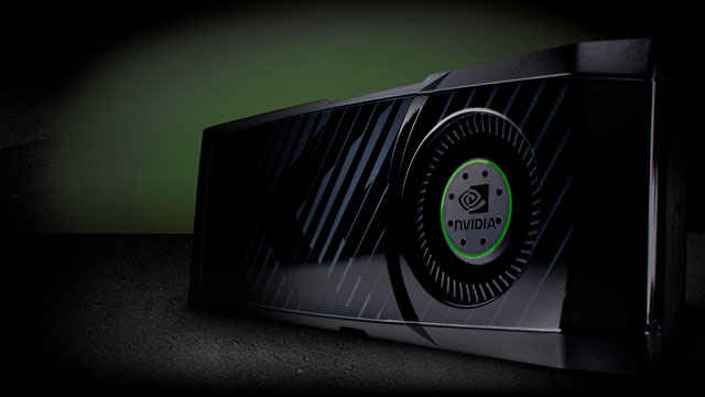
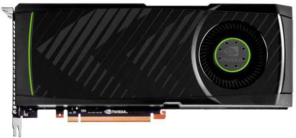
The Nvidia GeForce GTX 580 has been officially released, and aside from the reference card priced at $499 (the GTX 480’s abandoned price point), partner cards without custom cooling solutions or factory overclock settings are retailing for around the same price.
A whole heap of reviews have also piled in since the end of last night’s embargo, and all of them are unanimous with the verdict: the GTX 580 outperforms the GTX 480 in every aspect, and is everything the GTX 480 should have been when it released.
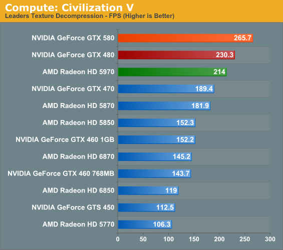
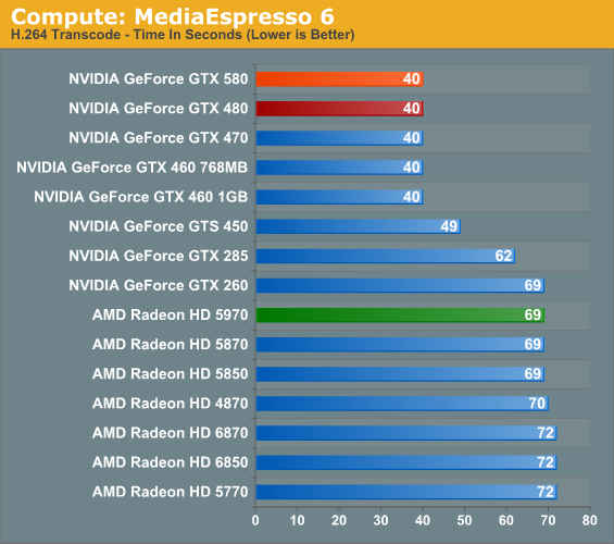
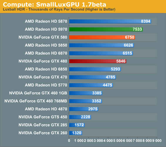
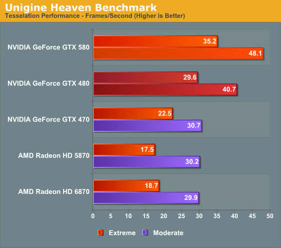
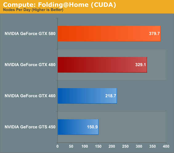
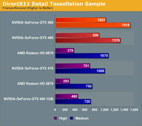
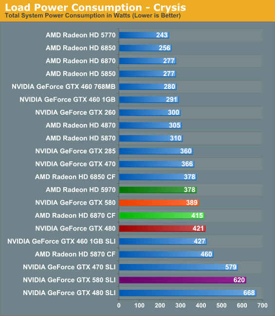
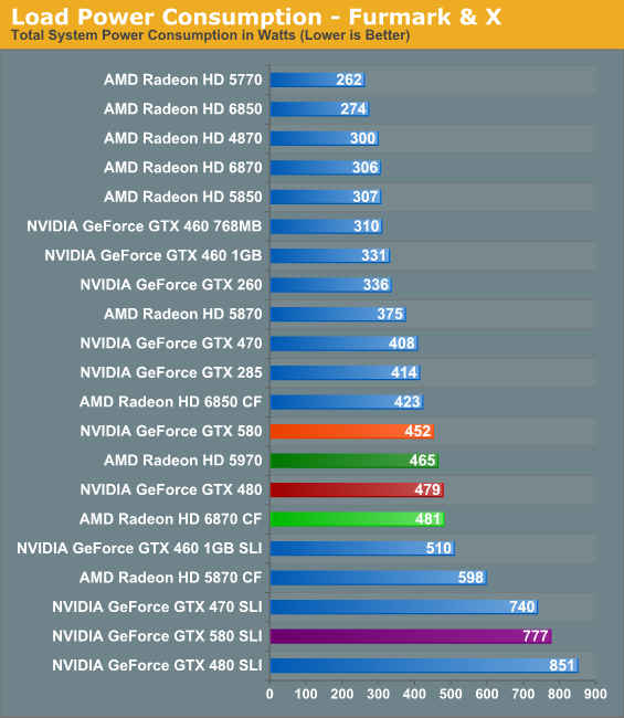
Some benchmarks have been posted on the next page, and you really should take a look to check out the performance improvement over the GTX 480, as well as how it competes against the HD 5870, HD 5970, and the HD 6870 CF. Do also check out detailed specifications on the next page.
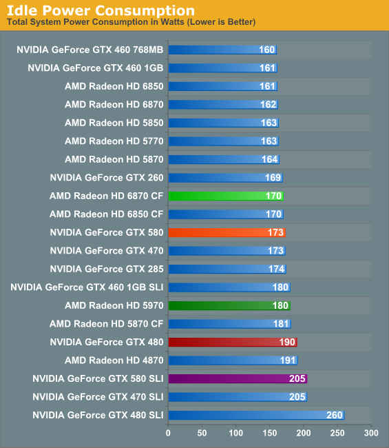
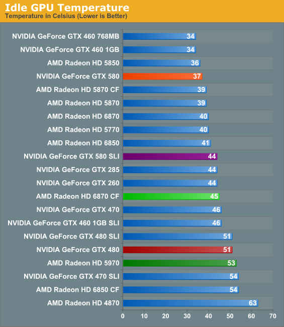
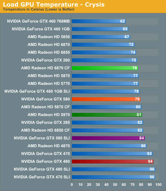
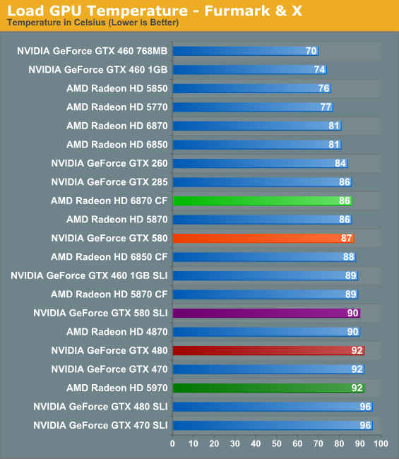
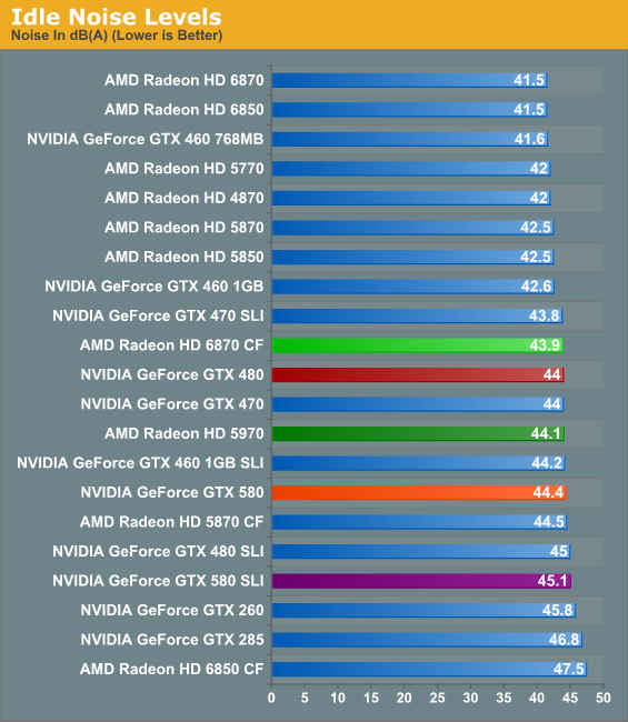
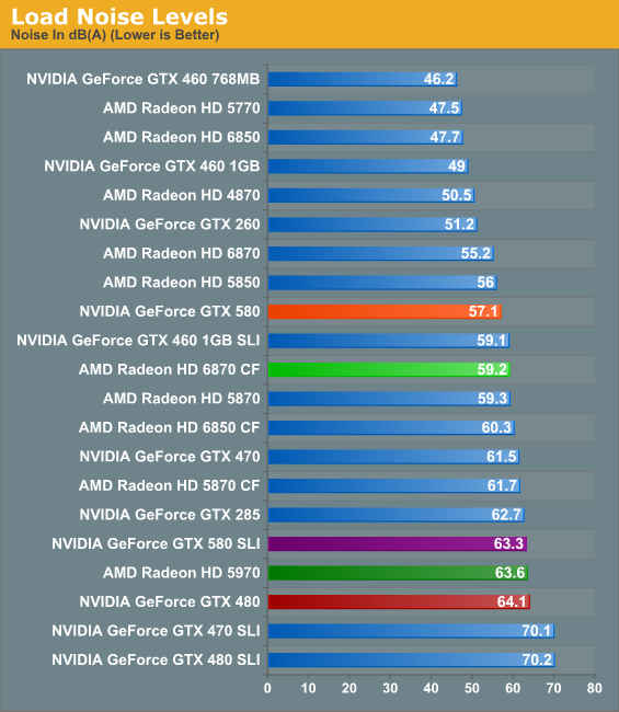
We already know about the new vapour-based cooling solution Nvidia has used in the GTX 580, and while this undoubtedly helped reduce the idle and load temperatures of the compared to its predecessor (and removes the GTX 480’s unsightly heat pipes), the GF110’s architecture has more tricks up its sleeve to account for its reduced power consumption and increased performance.
The world ridiculed the GTX 480 when it first arrived on the scene, grudgingly handing it the fastest DX11 single-GPU on the planet title, while complaining about its noise, temperature, and power consumption. Nvidia obviously had to do something to address the criticism its flagship GPU was facing, and it begun by working to refine the GF100’s architecture in future derivatives. The GTX 465 was one such GPU, based on the GF102 architecture, and offering better performance per watt figures. Then came the real performance value king, the GTX 460, which based on the much more refined GF104 architecture firmly set the crown of the most scalable performance per watt card in the market on Nvidia’s head, and, finally gave the much-vaunted yet to deliver Fermi architecture its due apart from producing a room heater.

The GTX 580’s GF110 architecture has taken many a learning from the GTX 460’s GF104 architecture, and incorporated it into the GF100 design. Structurally and constitutionally the GF110 architecture is virtually indistinguishable from the GF100 architecture, expect for the fact that none of the CUDA cores or stream processors are locked, possibly because of TSMC having worked out some of its flaws in the 40nm process, and, Nvidia having marginally reduced the die size. The entire L2 cache is also available, as well as all the ROPs. The memory bus (6×64-bit memory controllers), the memory (1.5GB GDDR5), and the transistor count (3 billion) all remain the same. The GTX 580 will also require both 6- and 8-pin connectors to power it, just like the GTX 480.
Differences however are found in the core, memory, and shader clocks, which have all been significantly increased, as well as in the texture hardware, which is obviously inspired by the GTX 460 and much improves the GF110’s texture filtering speed (per texture unit), at 32bit (INT8), 64bit (FP16), and 128bit (FP32).
One of the biggest improvements in design is brand new to the GF110 and the GTX 580, which is better Z-culling. This helps the GPU cull pixels that will never be seen in the final output, early on in the rendering process, thereby reducing workload and power consumption, and considerably speeding up performance (including tessellation), to up to 8% according to Nvidia.
[RELATED_ARTICLE]Among other important changes in design, the GTX 580’s fan has also met with some modifications for the better, namely a plastic ring incorporated to reduce instability and high-frequency noise, and a new airflow design, which will serve to make the card quieter and more efficient at cooling.
All this combines not only to give reduced noise, power consumption and operating temperatures, but up to 6.6% improvement in shading, texturing, and geometric performance than the GTX 480 at the same clockspeeds. Overall, improvements across the board are visible in the range of 10% to 30%, by various reviewing sites who got their hands on the ‘fasted DX11 GPu on the planet.”
How will all this compare with AMD’s offerings remains a very pertinent question, and in the benchmarks visible on the next page, some shocking stats do reveal themselves. A dual HD 6870 CrossFireX setup noticeably outperforms the GTX 580, for a combined price that is a bit lower. However, dual-GPU and CrossFireX/SLI results should be treated with care of course, as the load power consumptions will almost always be higher than a single GPU, as well as a greater disparity between minimum and maximum framerates. For now however, until the HD 6900 series rolls out (the dual-GPU [Antilles] HD 6990 is now rumoured to release only in Q1 2011), the GTX 580 definitely holds the crown of the “fastest DX11 GPU on the planet”, with much more grace than the GTX 480.
Read on to see benchmarks and specifications of the GTX 580…
|
|
GTX 580
|
GTX 480
|
GTX 460 1GB
|
GTX 285
|
|
Stream Processors
|
512
|
480
|
336
|
240
|
|
Texture Address / Filtering
|
64/64
|
60/60
|
56/56
|
80 / 80
|
|
ROPs
|
48
|
48
|
32
|
32
|
|
Core Clock
|
772MHz
|
700MHz
|
675MHz
|
648MHz
|
|
Shader Clock
|
1544MHz
|
1401MHz
|
1350MHz
|
1476MHz
|
|
Memory Clock
|
1002MHz (4008MHz data rate) GDDR5
|
924MHz (3696MHz data rate) GDDR5
|
900Mhz (3.6GHz data rate) GDDR5
|
1242MHz (2484MHz data rate) GDDR3
|
|
Memory Bus Width
|
384-bit
|
384-bit
|
256-bit
|
512-bit
|
|
Frame Buffer
|
1.5GB
|
1.5GB
|
1GB
|
1GB
|
|
FP64
|
1/8 FP32
|
1/8 FP32
|
1/12 FP32
|
1/12 FP32
|
|
Transistor Count
|
3B
|
3B
|
1.95B
|
1.4B
|
|
Manufacturing Process
|
TSMC 40nm
|
TSMC 40nm
|
TSMC 40nm
|
TSMC 55nm
|
|
Price Point
|
$499
|
~$420
|
~$190
|
N/A
|
 Crysis: Warhead
|
 Metro 2033
|
 |
 |
 |
 |
 |
 |
 |
 |
 |
 |
 |
 |
 |
 |
Benchmarks courtesy: AnandTech