GTC 2024: NVIDIA Blackwell, GB200, NVL72, SuperPODs, and more revealed

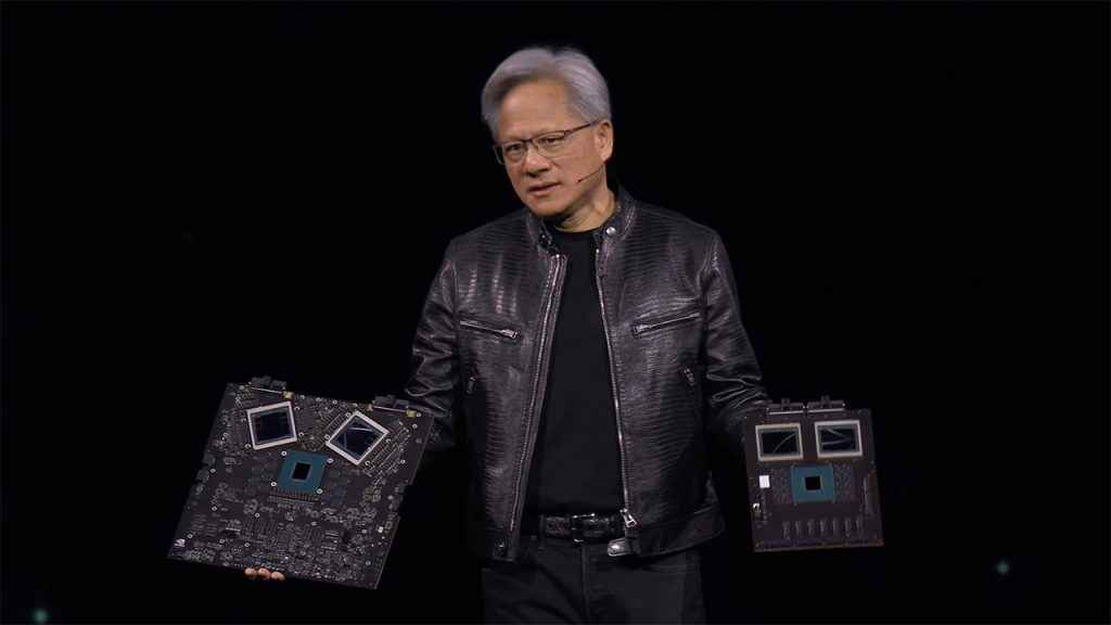
NVIDIA announced the dual-die B200 Blackwell GPU as a successor to their much sought after H100 and H200 Hopper GPUs. The new NVIDIA Blackwell B200 boasts a significant leap in computational power with over double the transistor count, 192 GB of HMB3e memory and 8 TB/s of bandwidth. The Blackwell B200 is a data-centre GPU and is expected to launch later in 2024. With startups such as Cerebras coming out with their WSE 3 ‘wafer scale’ GPUs that have much higher computational power, cores, memory bandwidth and interconnect bandwidth than NVIDIA H100, it becomes imperative for NVIDIA to continue to push out bigger and better chips despite its market leadership.
NVIDIA’s Blackwell GPU is named after Dr. David Harold Blackwell, an American statistician and mathematician who made significant contributions to probability theory, game theory and was also one of the three eponyms behind Rao–Blackwell–Kolmogorov theorem. NVIDIA hopes to continue the same momentum as the Hopper architecture and the Ampere architecture before it, with the introduction of the new Blackwell GPUs.
NVIDIA Blackwell goes the AMD way with MCM
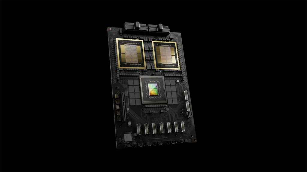
With the Blackwell B200, NVIDIA has gone the AMD way of introducing chiplets in their design. The Blackwell B200 is actually built by slapping together two GPU tiles with 104 Billion transistors, each. In comparison, the Hopper H100 had about 80 billion transistors. So the individual tiles have not scaled much but when you combine two tiles, you get a massive 208 billion transistors talking to each other using a 10 TB/s NV-HBI (NVIDIA High-bandwidth interface). NVIDIA Blackwell is built on TSMC’s 4NP processor node which is a slightly improved version of TSMC’s existing 4N node that’s being used for the Hopper H100 GPUs. Also, the 4N node is a 5 nm process and not a 4 nm process.
The reason NVIDIA had to resort to using chiplets like AMD does with their Instinct MI300 GPUs is because the H100 GPUs were already nearing the reticle limits of TSMC’s 4N process node. What this means is that the NVIDIA H100 GPU is one of the largest single GPUs that TSMC can make on a single silicon wafer. The H100 is 814 mm2 in size whereas the reticle limit is about 858 mm2. Therefore, scaling a chip requires the use of a multi-chip-module or MCM approach. And while NVIDIA Blackwell is a dual-chip GPU, NVIDIA does have something bigger planned to launch around 2025-26 called the GX200.
On the memory front, each Blackwell B200 die will use four HBM3e stacks of 16 GB that are connected to the GPU using a 1 TB/s interface. NVIDIA claims to have 20 petaflops of compute performance with the new Blackwell B200 GPUs but it should be noted that while all previous claims have been with FP8 precision, NVIDIA’s 20 petaflops is on a new FP4 precision. If we are to be fair, then the Blackwell B200’s compute performance would be around 10 petaflops with FP8. That’s more comparable to what most manufacturers use to indicate compute performance. And with FP8, the Blackwell B200 is only 2.5x times the performance of the H100 does 4 petaflops at FP8. All in all, NVIDIA’s B200 isn’t that big of a leap as the H100 as the H100 was over its predecessor. And most of it comes down to the limits of the process node.
Does that mean that the FP4 figure is nothing but hot air? Not quite. NVIDIA is using a new second gen Transformer Engine that can help convert AI models to utilise FP4 precision. And the NVIDIA Blackwell GPUs also support a new FP6 format as a go-between that offers a bit more precision than FP4 for models that can make do with slightly less precision than FP8.
Overall, NVIDIA is claiming to get a 4x increase in AI training performance and 30x increase in inference performance compared to the NVIDIA H100. Nvidia offers various Blackwell configurations, including the GB200 superchip with two B200 GPUs and a Grace CPU, offering up to 20 petaflops of FP4 AI inference per GPU. The HGX B200 and B100 configurations cater to different power and performance requirements, with the latter designed for compatibility with existing H100 infrastructure.
NVLink 7.2T
With new GPUs come faster interlinks. You have to put in faster interconnects otherwise all the compute improvements are of no use as they’d get bottlenecked. And interconnects are very expensive in terms of power and time, as resources. With Blackwell, NVIDIA is bringing out the fifth generation of NVLink and along with it, a new NVLink 7.2T switch.
The new NVIDIA NVLink 7.2T chip supports 7.2 TB/s of full-duplex bandwidth cumulatively. Each fifth generation NVLink interface has a max bandwidth of 1.8 TB/s and with four such NVLinks on one chip, the net bandwidth becomes 7.2 TB/s. The NVLink 7.2T chip is also built using TSMC’s 4NP process node and it supports 3.6 teraflops of Sharp v4 in-network compute on chip. SHARP (Scalable Hierarchical Aggregation and Reduction Protocol) comes from Mellanox which was acquired by NVIDIA. It is a technology that improves performance of large scalable HPC machines by offloading collective operations from CPUs and GPUs to networking chips.
NVIDIA B200 NVL72
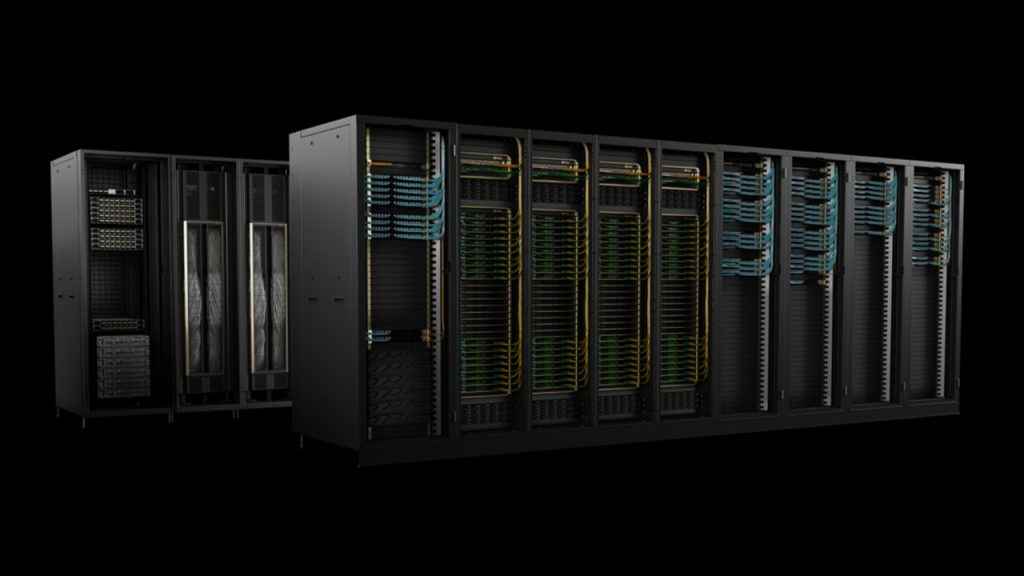
All of NVIDIA’s announcements clubbed together brings you the NVIDIA B200 NVL72, a massive GPU which is made of 18 1U servers that have two GB200 superchips, each. Each superchip is built using a single Grace CPU linked to two GB200 GPUs. This is unlike H100 which had a 1x CPU-1x GPU pairing. Each server will have two Grace GPUs and four NVIDIA Blackwell GPUs. That’s about 80 petaflops of FP4 performance. Each tray will also have two NVLink switches giving rise to a cumulative bandwidth of 14.4 TB/s.
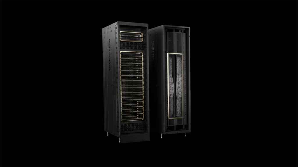
Overall, the NVIDIA GB200 NVL72 has 72 Blackwell GPUs, hence the 72 in the name. Along with that it gets 36 Grace CPUs, and 130 TB/s of cumulative bandwidth thanks to 18 NVLink switches. AT GTC 2024, NVIDIA also announced the SuperPOD which allows 576 GB200 Blackwell GPUs per domain.