AMD’s 14nm FinFET Polaris GPU Architecture Explained
AMD’s Polaris features their 4th generation Graphics Core Next (GCN) architecture, support for HDMI 2.0a and DisplayPort 1.3, and 4K H.265 encode/decode capabilities. So what exactly is the red giant bringing to the table?

AMD demonstrated their upcoming Polaris GPU architecture at CES 2016. The new 14nm FinFET architecture promises quite a few enhancements over the previous generation including HDR monitor support, improved power-efficiency, 4th generation Graphics Core Next (GCN) architecture, support for HDMI 2.0a and DisplayPort 1.3, and 4K H.265 encode and decode capabilities.
While AMD hasn’t released much information about the new architecture, let’s take a look at what all we know about the new 14nm FinFet Polaris Architecture.
What’s great about the 14nm FinFET Architecture?
While we aren’t going to school you as to how MOSFETs work but functionally it’s very simple. In a transistor – the most basic digital circuit – flow of current from the Source to Drain is controlled by the Gate. So better control of the Gate leads to better performance. This is as simple as we can put it.
Traditional transistors have been Planar i.e. you have multiple planar (flat) substrates with the topmost substrate being the Gate. As things existed in currently available silicon architecture, there was just one plane that was common between the Gate and Source-Drain in Planar transistors. In FinFETs, the Gate wraps around the Source-Drain so there are two planes in contact with the Gate. This small tweak is a big deal because it allows for a more finer control over the current flow. That’s essentially the manufacturing process that AMD’s implemented for the first time. It’s called a FinFET because the Gate looks like a fin protruding through the top.
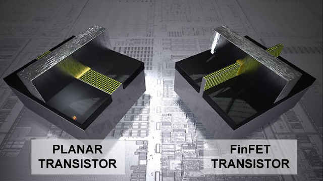
So how exactly is this new technology beneficial? Follow this chain of causation – since the FinFET design allows for twice as much Gate control vs Planar transistors, the current flow can be more accurately controlled. This results in less leakage current. So you can have a higher current level when the transistor is switched on and also consume much lower current during its off state. Essentially, you’re saving a lot of power by reducing leakage current. This brings down the heat generated by the GPU die and subsequently allows for low-TDP GPUs to be designed. TL;DR – Polaris will be a lot more power efficient.
To put things into perspective. Let’s take a look at Intel’s Broadwell architecture. The Desktop variants of Broadwell that had similar characteristics to their predecessor Haswell equivalents were rated for 19 W lesser. Example – The Haswell Core i7 4770 (3.4 GHz) was rated at 84 W and the Broadwell Core i7 5775C (3.3 GHz) was rated at 65 W. The socketed Broadwell has been since then touted as a hidden gem because the performance difference between the two was tremendous. However, don’t expect similar performance increment from Polaris GPUs. It could be much greater or slightly lesser, only time will tell – the first wave of GPUs are expected by mid-2016.
Dammit! What does all of this mean?
The obvious outcome of this new technology as with every other shrink in manufacturing process is that you’ll see more low-power laptops featuring a discrete GPU. And not just the thin low-power ones, even the beefy monstrosities that are ‘Gaming Laptops’ will end up being a lot more thinner since heat sink assemblies will be much smaller owing to the reduced TDP. And the same will be seen in Small Form Factor (Mini PCs) machines as well. Not to mention desktop graphics cards which will have fewer power connectors as they’ll give more performance per watt. This will allow for a higher adoption of mid-range and high-end graphics cards in price conscious markets like India.
4th generation Graphics Core Next (GCN) ahoy!
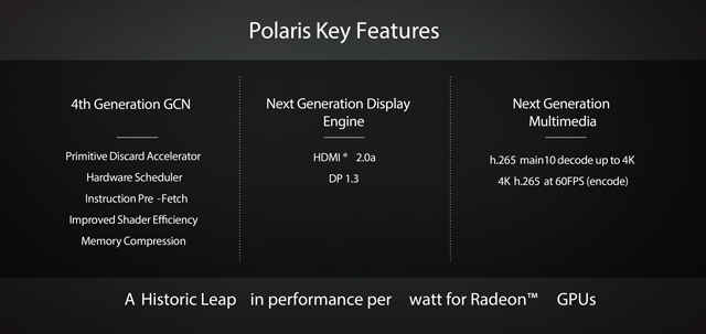
So key among the improvements that the 4th generation of Graphics Core Next (GCN) will feature involve the following:
Primitive Discard Accelerator
Polaris will support DirectX12 features like Conservative Rasterisation which would be used for occlusion detection, rendering curves and achieving transparency.
Hardware Scheduler
Improved handling of time / tick and executing whichever scheduling algorithm is in place.
Instructions Pre-Fetch
Instruction buffers have been increased. So more instructions can be scheduled in the pipeline or larger instruction sets can be pipelined before heading back to the nearest cache.
Improved Shader Efficiency
More texels / pixel fillrate / clock cycle. Translates to greater FPS towards the end of the GPU processing cycle.
Memory Compression
Data will be compressed before being sent via any transport bus. This allows for better bandwidth utilisation especially since High Bandwidth Memory (HBM) stacks opt for few high-bandwidth buses instead of more low-bandwidth buses.
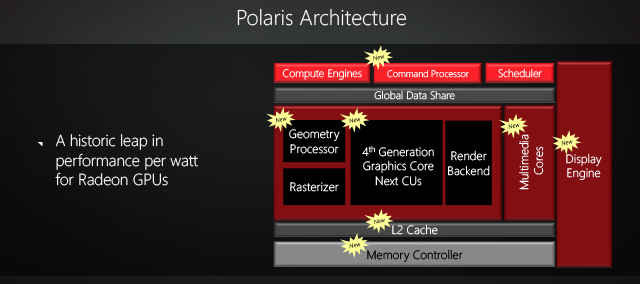
Next Generation Display Engine
So what kind of ports are we looking at with the Polaris.
HDMI 2.0a
This minor update to the HDMI 2.0 standard adds support for High Dynamic Range (HDR) content. HDR isn’t just a software add-on, though. While your old HDMI 2.0 cables will continue to work just fine with the new standard, you will require HDR supported monitors/TVs and source (graphics card / media box / streaming dongle, etc) devices. So if your new display supports HDR then prepare to be dazzled by a wider colour range and brighter whites in full 4K glory.
DP 1.3
DP 1.3 has been out since the end of 2014 but has now made its way onto graphics cards. This increases bandwidth from 21.6 Gbps on the DP 1.2 standard to 32.4 Gbps.
Next Generation Multimedia
So what kind of new encode / decode capabilities is Polaris capable of?
H.265 main10 decode up to 4K
H.265 is the next big video compression standard that will surpass the current H.264 standard or as it is more commonly known – AVC / MP4. H.265 offer twice the data compression ratio than H.264 without hampering video quality. Anything that promises a 100% higher compression ratio comes with a signification compute overhead and that means more graphics horsepower is needed. And each compression standard has multiple compression profiles with varying levels of quality between them. The Main10 profile allows for a colour depth between 8-bit and 10-bit. This is the higher end of the spectrum. Add to this the fact that H.265 can handle 8K content and you’re looking at a lot of data… that needs to be compressed… on the fly. But we’re limited to 4K with the Polaris architecture.
4K H.265 encode at 60 FPS
This is just an extension of the above feature. AMD’s Fiji architecture has support for H.265 too, except it is limited to 8-bit colour depth and Polaris takes it a step further.
So how does all of this affect my gaming experience?
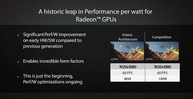
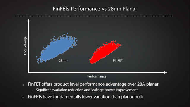
The most exciting thing that has everyone jumping up and down in joy happens to be the significant performance / watt improvement. AMD demonstrated their Polaris Engineering Sample with one of the most popular AAA titles out now – Star Wars: Battlefront. More specifically, they ran an X-Wing sequence with V-sync on. So while this did limit the FPS to 60, it highlights the power consumed to hit that threshold. AMD’s Polaris GPU consumed 86 watts while the NVIDIA GTX 950 consumed 140 watts. So Polaris consumes about 40% less power to do the same work. It is worth noting that EA’s Star Wars: Battlefront does not use NVIDIA Gameworks.
These figures were released by AMD and the benchmark was done on a rig consisting of:
- CPU – Intel Core i7 4790K
- Motherboard – ASUS H97I-PLUS
- RAM – 16 GB (4x 4 GB) DDR4-2600 MHz
- OS – Windows 10 64-bit
- Storage – 120 GB SSD
- Settings – Medium Preset
- Resolution – 1080p
- V-Sync – ON
- GPU – AMD Polaris Sample vs NVIDIA GTX 950
- Drivers – AMD 10.16 Beta, NVIDIA 359.06.
- Game – Star Wars: Battlefront
What do we think?
Everything that we saw today was based off one of the early engineering samples. However, AMD has a history of not releasing information to the public before working out all the kinks in the design. So it’s a little difficult to opine if these performance figures will be what the final products will ship out with. And then again, we’ve been hearing rumours of AMD’s next gen GPUs and CPUs having already been taped out. So the most logical conclusion is that when Polaris GPUs will hit the market later this year, it will either be the same or better.
Going by the last two GPU series that were launched by AMD, i.e. the Rx 300 and Rx 200 series, there were a lot of rebadged GPUs. This is a common strategy followed by the competition as well. So the entire line-up can be expected to have a mix and match of current and previous generation of GPUs with GDDR5 and HMB memory. Lower SKUs are likely to be rebadged Rx 300 or Rx 200 series GPUs with GDDR5 memory. Mid-range SKUs will likely comprise of old rebadges, a few Fiji GPUs with HBM and two or more Polaris GPUs (one with GDDR5 and the other with HBM).
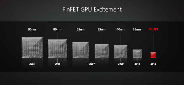
The FinFET process has matured quite well and there have been plenty of flagship launches since early 2015. This includes Intel’s Core M family (Core M 5Y10 / 5Y10a / 5Y70), Samsung’s 14nm Exynos on the Galaxy S6 and S6 Edge and Apple’s 14nm and 16nm A9. It’s likely that AMD will be going with TSMC for Polaris as well so there shouldn’t be any untoward production bottlenecks. Though we do believe that the initial batch will be limited so expect a minor price surge within weeks of launch.
AMD didn’t release any information about the number of Stream Processors that the Polaris Engineering Sample had. But it will be fun to see a Polaris GPU with 4096 Stream Processors go head to head with the NVIDIA TITAN X. The fact that Polaris has DisplayPort 1.3 could indicate that we might end up seeing 8K content. That’ll redefine overkill. We can’t wait to get our hands on a review sample. Stay tuned for more on this.