![ASUS F1A75-V Pro Llano motherboard [Preview]](https://static.digit.in/default/artImg75x64_7113.jpg "ASUS F1A75-V Pro Llano motherboard [Preview]")
Very recently AMD revealed its Llano line of A series Fusion APUs which will directly combat Intel’s Sandy Bridge. This new Socket FM1 A75 chipset makes for a very interesting value proposition considering that the integrated GPU on this processor (AMD likes calling the chip an Accelerated Processing Unit) is from the good ‘ol Redwood lineage. We’re talking HD 5670 level graphics on an integrated chip. Hence this could very well be the first time we’ll be seeing a decent graphics solution (for gaming, not just encoding/rendering) pushed onto a single chip. Also we’re hearing news of the integrated graphics units being overclocked to mind boggling heights. All of this makes us eagerly await the first few of these APUs to be shipped to India. Meanwhile, boards for the A75 Llano chipset have already started making inroads. Here we do a preview of the first board of its kind to come to our test center – ASUS’s F1 A75-V Pro – and in effect get you acquainted with this chipset and what it has to offer. Lets start with the package and bundle.
Package and Bundle
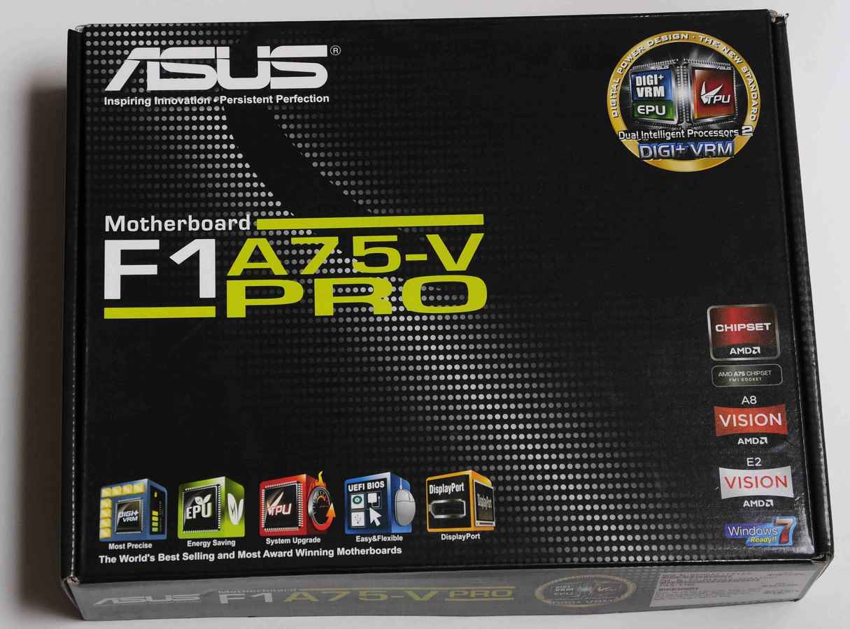
As you can see from the package, it follows pretty much the standard information outlay that we’re accustomed to for any of ASUS’s pro series boards. You’ve got logos for specific standards and features such as Vision and UEFI etc.
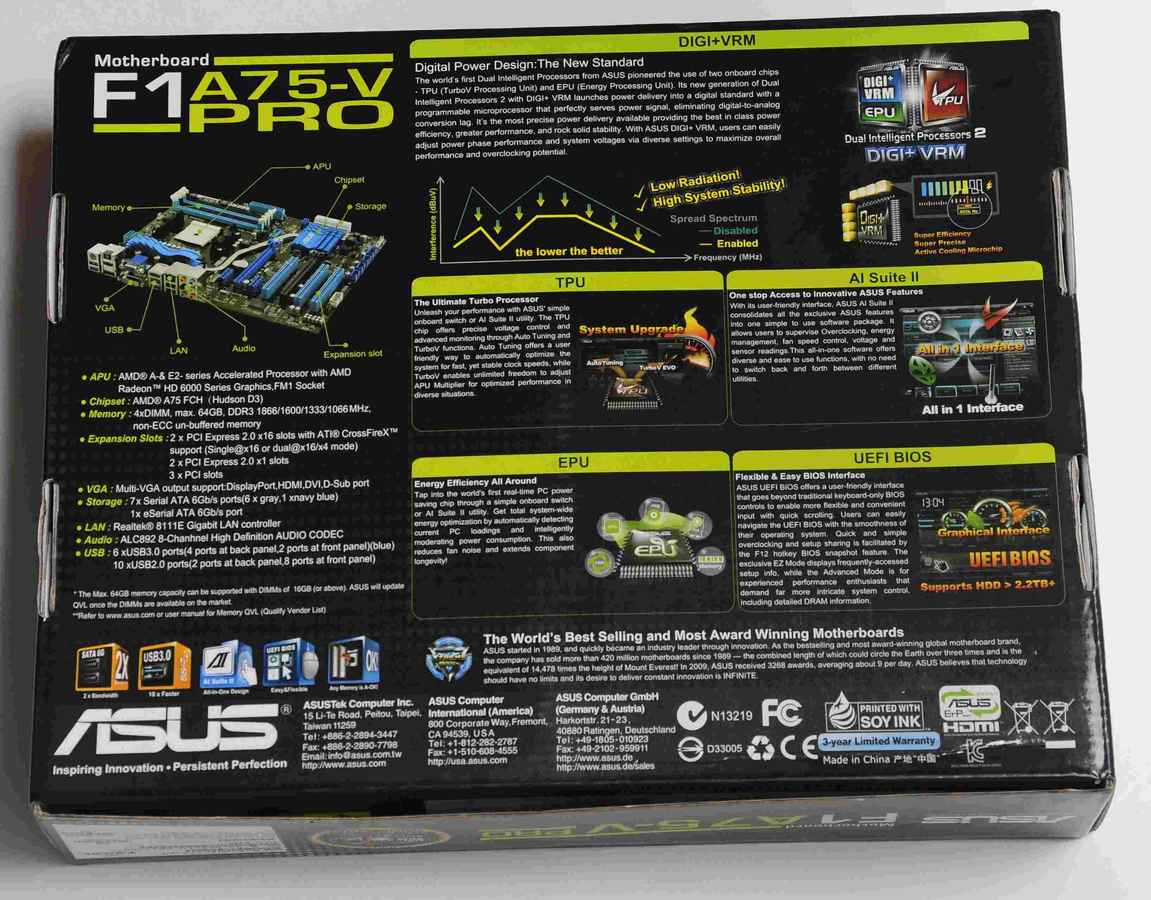
The back explains some of the features in more detail. The most interesting of these were the TPU and EPU boxes which we will talk about in a bit once we focus on those particular chips and what they do.
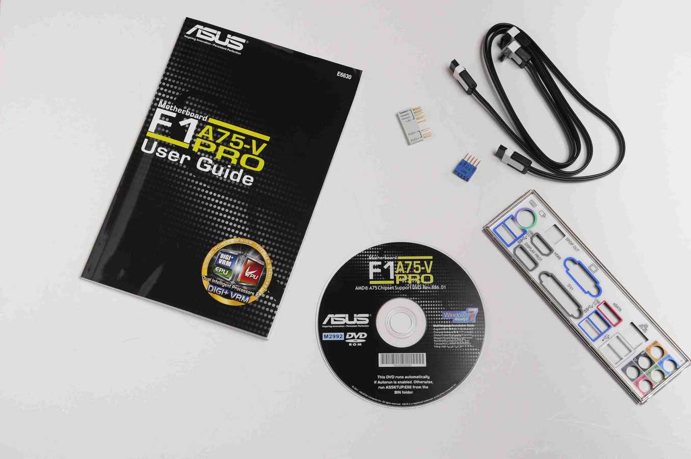
Inside the bundle we have a couple of things as expected. The Manual, Driver CD, couple of connectors, two SATA cables and the I/O panel shield. The IO shield in fact was interesting in a way that it had a soft sponge back, which is not something we’ve seen. The sponge allows for nice play when mounting the board in a case.
Click next to read more about ASUS’s F1 A75-V Pro motherboard….
Now for the board itself
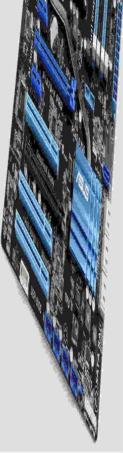
The colour scheme on the board – a cool blue and black – is again in line with the Pro series from ASUS. One of the things that will instantly be noticed is the heatsink design. We suppose apart from just aesthetics those wavy fins allow for more dissipation. Two of these chunky heatsinks are connected by a heat pipe. One is next to the FETs and one covers the chipset or southbridge.
Next we have the expansion slots. The set up includes seven slots in the following configuration: Three PCI, Two x1 PCI-E, and Two x16 PCI-E. However one of the x16 slots will only give speeds of upto x4 since it’s been wired to support as much.
On the other half of the board we find the four DIMM slots. The slots support up to 64 GB of DDR3 RAM clocked at upto 1866MHz (yeah, we were surprised too. But ASUS will update QVL once the DIMMs of 16GB are available in the market). Next to the 24 pin main power connector you have the MemOK button as well as the TPU and EPU switches. Next to the DIMM slots (on the left) you find the USB 3.0 header (in blue). The chipset has provision for a native USB 3.0 controller, so, apart from the two USB 3.0 ports in the back panel this header will allow for connecting to two more on the front panel of the case.
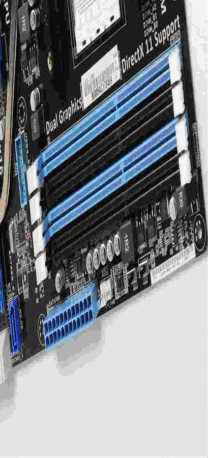
Coming to the IO ports, we have a whole lot of things. You are sure to catch the 4 USB 3.0 ports – two below the PS/2 combo and two below the eSATA port. That means using the header, you can have upto 6 USB 3.0 ports. In the display department you have an option between four ports – HDMI, Display Port, VGA and DVI. For audio you have a standard 6 port configuration. The LAN port is Gigabit while the two USB ports 2.0 ports are two of 10 that the chipset can support.

Click next to read more about ASUS’s F1 A75-V Pro motherboard….
The socket that you see is the Socket FM1 that features a new cooling bracket.
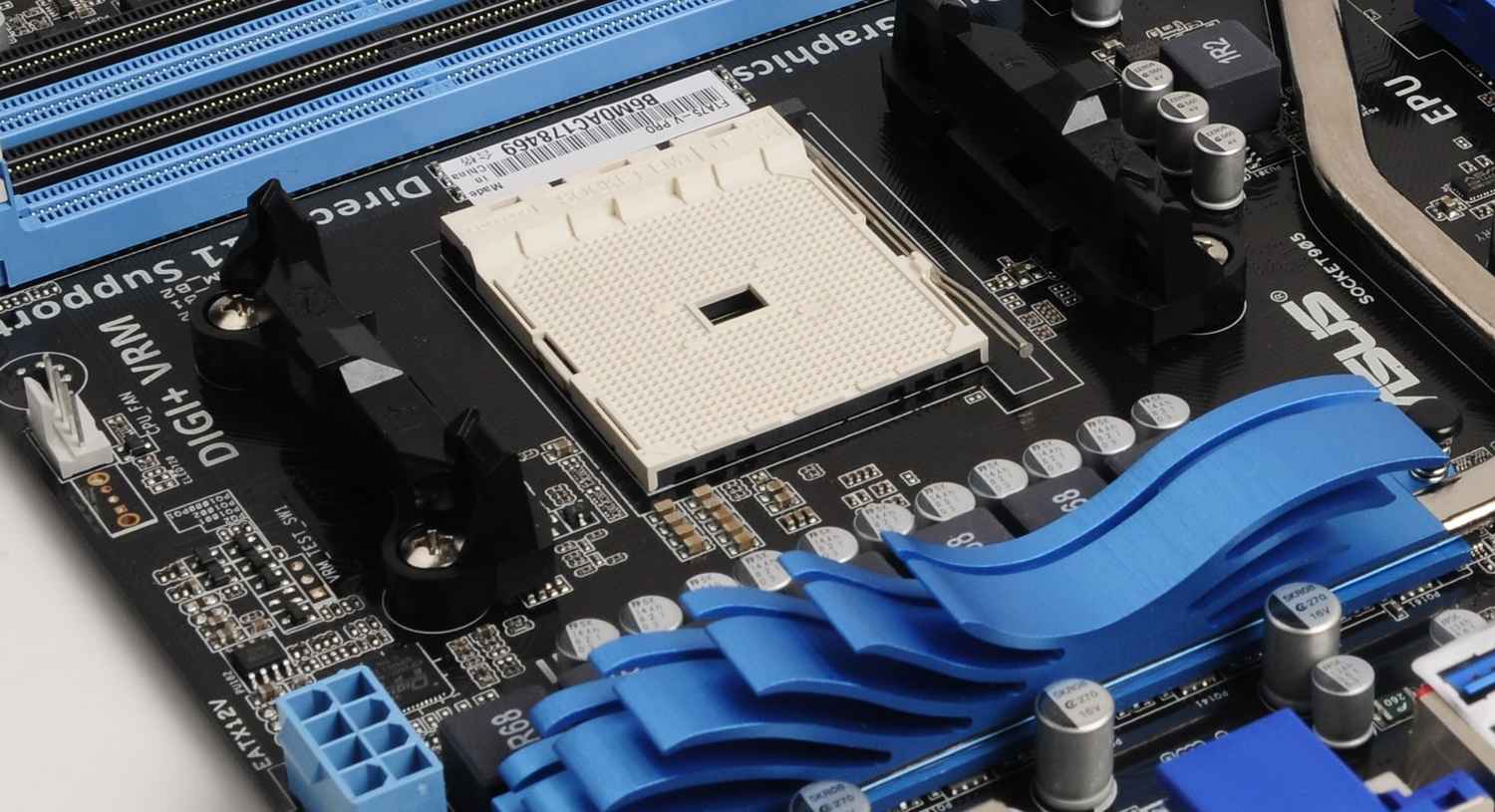
The six SATA ports on the board are all 6Gbps which is an advantage with Intel’s usual configuration on Sandy Bridge Series 6 chipsets of two 6 Gbps and four 3 Gbps.

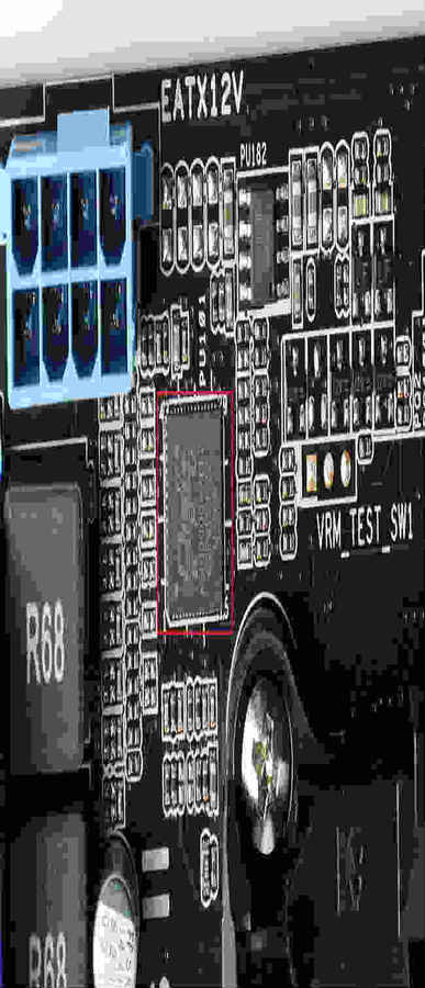
And now finally we come to the two switches that we spoke of earlier – the EPU (Energy Processing Unit) and TPU (TurboV Processing Unit). What you see below are the controller chips for these two features. Both can be controlled from the BIOS but the board provides physical switches too. The EPU is a power management chip that is supposed to intelligently moderate power consumption by automatically detecting PC loads.
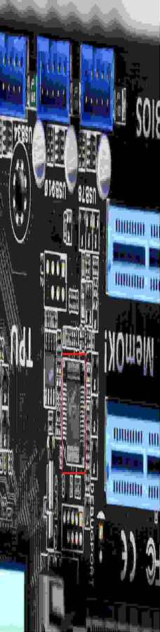
The TPU is a performance controller that relates to overclocking tweaks. The chip offers a higher level of voltage control and monitoring. Auto Tuning is a feature that offers a way to automatically boosts speeds while keeping the system stable. TurboV allows you to manipulate the APU multiplier.
So that’s it for our preview. Stay tuned for performance benchmarks and a full review once we get our hands on the APU.
Siddharth Parwatay
Siddharth a.k.a. staticsid is a bigger geek than he'd like to admit. Sometimes even to himself. View Full Profile


